Basic Min/Max Analysis Sets Resistor Values for Photocoupler Circuit
Download this article in PDF format.
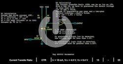
Determining the resistor values and assuring performance of the circuit associated with a photocoupler (also called an optocoupler or optoisolator) is simple in principle, but there are some points to consider when creating a robust, trouble-free design. Using an example based on the Renesas PS8902 (a high-speed, analog-output photocoupler with a GaAlAs LED on the input side, and a PIN photodiode and high-speed amplifier transistor on the output side), it’s illustrative to do the calculations for resistor selection and drive, The schematic “fragment” of the figure summarizes the analysis scenario.
This “fragment” of a larger schematic shows the key aspects of the phototransistor input drive and output circuit, which are needed for the resistor and current analysis.
First, the actual power rails may not be at 5.0 V and 3.3 V, even though the schematic says that’s the case. Instead, it’s important to know how far “off” they can be from those nominal values. In this example, assume the power supplies are within ±10%, which means they can be as low as 4.5 V and 3.0 V, respectively. Begin by calculating the value of input resistor R1 after picking a suitable forward current IF for the emitting diode. A good starting value is 5 mA, as that that won’t overstress the diode or cause it to age too quickly.
Closely reading the PS8902 datasheet indicates that emitter forward voltage VF can be as high as 1.85 V:

As the emitter isn’t being driven with 16 mA, VF will very likely be lower, but the 1.85-V value is sensible and provides some margin. The voltage available to drive the emitter is the supply voltage minus VF and the driver VF, which in this case is assumed to be zero (which is close enough for this FET driver), so
R1 = (VCClow − VF) / IF
R1 = (4.5 V − 1.85 V) / 0.005 = 530 ≅ 536 Ω (the closest standard value)
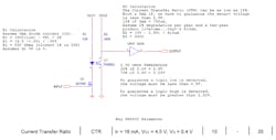
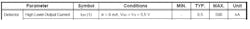
The emitter current of 5 mA is coupled to the output via the current transfer ratio (CTR), which the datasheet states can be as low as 15%, so that 5 mA of current can be as low as 750 µA:

CTR degrades over time, and the amount of degradation depends on the operating environment and how “aggressively” the emitter is driven (in this example, it is not being very hard). A safe estimate for degradation is 2% per year. For this example, assuming the expected operating lifespan for the design is 10 years, a degradation of 2% per year for 10 years reduces the output current from 750 µA to 610 µA.
The challenge is to make sure the logic gate recognizes the ON state, which means the logic-gate voltage must be below 30% of the low VCC rail, or 0.9 V. With 610 µA flowing through R2 and requiring less than 0.9 V at the gate input, this leaves 2.1 V to drop across R2:
R2 = V/I = 2.1 V/610 µA = 3400 Ω
There’s one more thing to check before “signing off” on this design, and that’s to ensure the leakage current in the detection transistor, with the voltage drop across R2, yields a gate voltage that will still be detected as logic high:
The voltage drop is only 1.7 mV with 500 nA flowing through R2, so there won’t be a problem keeping the gate voltage above 2.52 V.
As indicated at the beginning, this isn’t a complicated design process, but there are a few important things to keep in mind when doing it.
About the Author
Ken Coffman
Senior Principal Field Applications Engineer
Ken Coffman is a Senior Principal Field Applications Engineer for Renesas Electronics America. He received his B.S. in Electrical Engineering from Cogswell College North (Wash.).
Comment About the Article
To join the conversation, and become an exclusive member of Electronic Design, create an account today!

Leaders relevant to this article: