Enhance Power-Delivery Efficiency for Demanding AI and Data Center Apps

What you'll learn:
- Insight into ASE's powerSiP technology.
- How the technology differs from traditional power-delivery systems.
A new power-delivery platform from Advanced Semiconductor Engineering (ASE) is designed to increase power efficiencies while reducing signal and transmission loss. The company states its powerSiP voltage regulator module (VRM) addresses density challenges with a 50% increase in current density from 0.4 to 0.6A/mm² and a decrease in routing power loss from 12% to 6%, facilitating a 50% reduction over those with a side-by-side configuration.
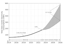
The powerSiP technology is ASE’s answer to the continuous rise of compute power and cooling—the two most energy-intensive processes in data centers. According to a 2024 report from Berkeley Labs, U.S. data center electricity use remained stable until 2017. However, due to the rise of GPU-powered servers for AI, that consumption has ramped up, reaching 176 TWh in 2023 (4.4% of national consumption).
Projections estimate data center energy use could climb to between 325 and 580 TWh by 2028 (Fig. 1), which translates to 6.7% to 12% of total U.S. electricity consumption. Traditionally, efficiency improvements made that energy use steady, but AI hardware growth ended that trend, with energy demand now increasing rapidly.
As AI and data centers continue to evolve, the efficiency of power-delivery networks (PDNs) becomes crucial. While individual power-conversion stages offer efficiency in the mid-to-high (90%) range, routing losses can act as a bottleneck as those levels rise. This is often shown when it comes to DC-DC converters connected to microprocessors.
Traditional systems have often relied on a single-stage voltage-reduction approach to mitigate that challenge, providing power to the microprocessor at a higher voltage using the VRM. The powerSiP platform, on the other hand, takes advantage of a multi-stage, VRM-based PDN solution, which enhances overall system efficiency without requiring higher voltages.
powerSiP's Vertically Integrated Design
Unlike side-by-side configurations, powerSiP features a vertically integrated design, placing the VRM directly under the SoC or chiplets (Fig. 2). The design reduces the distance for power delivery, thus lowering impedance and improving power efficiency.
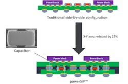
The multi-stage VRM approach ensures efficient voltage regulation tailored to the specific needs of high-performance applications. By going vertical, and embedding inductors/capacitors directly into the packaging, shortens the power-delivery path, which improves efficiency. It also places the voltage regulation inside the package or very close to it, instead of relying on distant motherboard components, helping reduce energy loss.
Packaging is another key factor in powerSiP’s cooling and energy efficiency, as the modules employ advanced packaging techniques, such as fan-out chip-on-substrate (FOCoS-B). The technology also uses embedded inductors that are fabricated directly into the substrate or fan-out layers, which shrink the footprint and increase performance.
"System efficiency is a top priority for architects, particularly as the world explores ways to address the growing global demand for electricity at the same time as driving down carbon emissions," stated Patricia MacLeod, Senior Director of Corporate Communications & Industry Partnerships at ASE. "Our powerSiP platform signifies another step forward for ASE in our endeavor to help enable more efficient power solutions and greener data center energy utilization that aligns with our corporate commitment to sustainability."
About the Author

Cabe Atwell
Technology Editor, Electronic Design
Cabe is a Technology Editor for Electronic Design.
Engineer, Machinist, Cartoonist, Maker, Writer. A graduate Electrical Engineer actively plying his expertise in the industry and at his company, Gunhead. When not designing/building, he creates a steady torrent of projects and content in the media world. Many of his projects and articles are online at element14 & SolidSmack, industry-focused work at EETimes & EDN, and offbeat articles at Make Magazine. Currently, you can find him hosting webinars and contributing to Electronic Design and Machine Design.
Cabe is an electrical engineer, design consultant and author with 25 years’ experience. His most recent book is “Essential 555 IC: Design, Configure, and Create Clever Circuits”
Cabe writes the Engineering Life & Engineering on Friday blog on Electronic Design.
See Cabe's cartoons & comic strips here.
Comment About the Article
To join the conversation, and become an exclusive member of Electronic Design, create an account today!

Leaders relevant to this article: