PowerPAK 8x8SW Package Promotes Cool-Running, Low-Loss 80-V MOSFETs
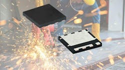
The SiEH4800EW 80-V TrenchFET Gen IV n-channel power MOSFET developed by Vishay leverages a PowerPAK 8x8SW bond wireless (BWL) package to enhance thermal performance and lower losses. With on-resistance down to 0.88 mΩ (typical) at 10 V, the device minimizes conduction-related power losses while improving thermal performance with a low maximum Rth(J-C) of 0.36 °C/W and operation to +175°C.
These characteristics suit the MOSFET for synchronous rectification and OR-ing functionality in applications such as motor-drive controls, power tools, welding equipment, plasma cutting machines, battery-management systems, robotics, and 3D printers.
The MOSFET’s TO-263 package has an 8- × 8-mm footprint (roughly 50% less than most comparable MOSFETs) and an ultra-low profile of 1 mm. The packaging also features a fused lead that increases the source PAD solderable area to 3.35 mm2 (4X larger than a traditional PIN solder area), decreasing the current density between the MOSFET and PCB. This reduces the risk of electromigration and enables a more robust design.
Samples and production quantities of the SiEH4800EW are available now, with lead times of 13 weeks. Additional technical information is available here.
Next in This Edition of PowerBites

More PowerBites


About the Author

Lee Goldberg
Contributing Editor
Lee Goldberg is a self-identified “Recovering Engineer,” Maker/Hacker, Green-Tech Maven, Aviator, Gadfly, and Geek Dad. He spent the first 18 years of his career helping design microprocessors, embedded systems, renewable energy applications, and the occasional interplanetary spacecraft. After trading his ‘scope and soldering iron for a keyboard and a second career as a tech journalist, he’s spent the next two decades at several print and online engineering publications.
Lee’s current focus is power electronics, especially the technologies involved with energy efficiency, energy management, and renewable energy. This dovetails with his coverage of sustainable technologies and various environmental and social issues within the engineering community that he began in 1996. Lee also covers 3D printers, open-source hardware, and other Maker/Hacker technologies.
Lee holds a BSEE in Electrical Engineering from Thomas Edison College, and participated in a colloquium on technology, society, and the environment at Goddard College’s Institute for Social Ecology. His book, “Green Electronics/Green Bottom Line - A Commonsense Guide To Environmentally Responsible Engineering and Management,” was published by Newnes Press.
Lee, his wife Catherine, and his daughter Anwyn currently reside in the outskirts of Princeton N.J., where they masquerade as a typical suburban family.
Lee also writes the regular PowerBites series.
Comment About the Article
To join the conversation, and become an exclusive member of Electronic Design, create an account today!

Leaders relevant to this article: