Could This “2D” Transistor Process Transform Logic and Power Device Production?
What you'll learn:
- CDimension’s technology, which enables semiconductor makers to manufacture arrays of extremely small, fast, and efficient “2D” transistors, has the potential to change what’s possible for both digital and power devices.
- The technology can be used to form a single layer of 2D transistors, or multiple layers of vertically integrated devices is compatible with standard COMOS processes.
- The company said it’s already helping several chipmakers explore how to apply the technology to produce digital and analog ICs with dramatically higher logic densities, operating speeds and energy efficiency.

CDimension recently unveiled a technology that enables conventional semiconductor fabs to use ultra-thin semiconductor materials to manufacture vertically integrated arrays of extremely small, fast, and efficient “2D” transistors. It has the potential to change what’s possible for both digital and power devices.
According to the company, it’s already helping several chipmakers explore how to apply their technology to produce digital and analog ICs that offer dramatically higher logic densities, operating speeds, and energy efficiency.
CDimension is also providing developers with resources that will eventually enable them to use the same process to produce vertically integrated chips that unify compute, memory, and power functions within a single, high-efficiency device.
BEOL Process Enables Atomically Thin Film Growth
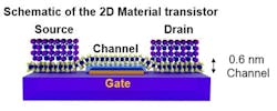
At the core of the company’s commercial debut is a proprietary, low-temperature, back-end-of-line (BEOL) process, which enables the direct growth of highly uniform, atomically thin (6 nm/3 atoms thick) films of materials, such as molybdenum disulfide (MoS2), onto a silicon substrate.
That layer can be processed using existing photolithographic processes to create transistors with much higher electron mobility (around 400 cm2/V/s), lower leakage and parasitic capacitance, and wider bandgaps (2.4 eV) than an equivalent CMOS device (Fig. 1).
Due to their thin structure and the absence of isolation wells, the resulting transistors also display significantly lower leakage and parasitic losses than their equivalent CMOS counterparts. As a result, internal testing of the so-called 2D devices fabricated in CDimension’s MoS2 films have demonstrated up to a 1,000X improvement in transistor-level energy efficiency compared to silicon.
Moving From Lab to Fab
To help early adopters explore the technology, CDimension offers 4- and 8-in. silicon wafers with a MoS2 film applied to them. Manufacturers can use these wafers to form 2D transistors using standard photolithographic processes available on most commercial 150- to 180-nm fab lines. This includes interconnects formed using a standard CMOS-compatible metallization layer such as copper.
The short distances and low parasitics displayed by these interconnects contribute to the devices’ high performance. Even better ohmic contacts can be achieved with bismuth, antimony, and nickel, but using these would require additional process steps.
CDimension said that it expects early adopters will use these single-layer MoS2-coated wafers to produce components such as low-power, high-speed MCUs, memories, and other digital devices. Other applications would be power devices that exhibit many of the advantages of wide-bandgap (WBG) materials such as gallium nitride (GaN) and silicon carbide (SiC).
Furthermore, the company noted that the technology has good potential for RF and sensing applications, and possibly quantum computing (with different materials).
A 3D Future?
Since the film deposition process is performed at 200°C, it can be used to create multiple layers of 2D devices and their associated interconnects without damaging the previously formed devices.
According to CDimension, this capability will eventually enable designers to create single-chip products that incorporate multiple layers of high-speed/low-power logic, memory, and other functionality, as well as high-density devices like MCUs with large, on-chip memories that are accessed through extremely short, low-resistance interconnects (Fig. 2).

When used to fabricate power devices, the resulting transistors can operate reliably at 40 to 45 V, are less susceptible to noise, and have switching speeds that are relatively voltage independent. CDimension said it’s confident that the channel length of these 1st-gen transistors can be adjusted to support higher voltages (100 V or less). Initial applications for 2D power devices could include high-efficiency, low-noise step-down regulators, especially for GPUs.
The first commercial applications for the technology are expected to hit the market in mid-2026, most likely small MCUs with integrated memory and power-management units (PMUs) for high-performance CPUs, GPUs, and SoCs.
>>Check out the TechXchange for similar articles and videos

About the Author

Lee Goldberg
Contributing Editor
Lee Goldberg is a self-identified “Recovering Engineer,” Maker/Hacker, Green-Tech Maven, Aviator, Gadfly, and Geek Dad. He spent the first 18 years of his career helping design microprocessors, embedded systems, renewable energy applications, and the occasional interplanetary spacecraft. After trading his ‘scope and soldering iron for a keyboard and a second career as a tech journalist, he’s spent the next two decades at several print and online engineering publications.
Lee’s current focus is power electronics, especially the technologies involved with energy efficiency, energy management, and renewable energy. This dovetails with his coverage of sustainable technologies and various environmental and social issues within the engineering community that he began in 1996. Lee also covers 3D printers, open-source hardware, and other Maker/Hacker technologies.
Lee holds a BSEE in Electrical Engineering from Thomas Edison College, and participated in a colloquium on technology, society, and the environment at Goddard College’s Institute for Social Ecology. His book, “Green Electronics/Green Bottom Line - A Commonsense Guide To Environmentally Responsible Engineering and Management,” was published by Newnes Press.
Lee, his wife Catherine, and his daughter Anwyn currently reside in the outskirts of Princeton N.J., where they masquerade as a typical suburban family.
Lee also writes the regular PowerBites series.
Comment About the Article
To join the conversation, and become an exclusive member of Electronic Design, create an account today!

Leaders relevant to this article: