Bandwidth or Function? What to Focus on When Designing High-Density Circuits
What you'll learn:
- The three bandwidth-related strategies that can yield results.
- How and why to take a bandwidth approach.
- Some of the methods for implementing a bandwidth-optimized approach.
As PCB feature sizes shrink and component packages grow more capable, it’s tempting to view circuit density primarily as a layout problem emphasizing finer traces, smaller vias, and tighter clearances. In practice, however, architecture-level decisions often determine whether a dense design is elegant or tortured.
By rethinking how circuits are grouped, how data moves, and where logic lives, designers can achieve substantial gains in circuit density, signal integrity, and manufacturability — often all at the same time.
One potential solution to the density problem lies in partitioning circuits by bandwidth and signal sensitivity rather than positioning them based on their function, which is the traditional approach. Further gains in circuit density can then be achieved by replacing wide parallel buses with serial links and consolidating “glue logic” into configurable devices.
However, each strategy comes with its own challenges and complexities, which are useful to understand before getting started.
How Can a Design be Partitioned by Bandwidth, Not by Function?
Traditionally, boards have usually been partitioned by functional blocks: the power supply, processor, memory, I/O, analog front end (AFE), and so on. While intuitive and simple, this approach often forces high-speed or noise-sensitive signals to traverse long distances, crossing multiple domains and layers. The result is congestion, excessive vias, and the need for routing “detours” that inflate the PCB’s overall area.
From a power density perspective, long high-speed routes become a significant bottleneck: They require wider spacing, reference plane continuity, controlled impedance, and aggressive length matching. Every additional millimeter constrains adjacent routing.
One alternative is to adopt a bandwidth-first principle. Partitioning the design by bandwidth means placing circuits according to the speed, sensitivity, or noise generation of their signals, regardless of the role they play in the system. As a result, the fastest or most timing-critical loops are made physically compact — even if this disrupts how traditional designs are crafted.
>>Download the PDF of this article
There are several drivers for the bandwidth-first strategy, including:
• Signal integrity: Shorter interconnects reduce loss, skew, and crosstalk.
• Electromagnetic coupling: Tight clusters allow local containment of high dI/dt and dV/dt.
• Routing efficiency: Compact high-speed regions free global routing space for slower nets.
Engineers can take several approaches to implement things in a bandwidth-first way, including:
• MCU + external memory: Place DDR, QSPI, or SRAM directly adjacent to the processor, even if it intrudes into the “power” or “I/O” region.
• ADC + driver + reference: Treat the signal chain as a single physical island, rather than scattering elements by function.
• Switching regulators: Keep the high-frequency power loop tight, even if it overlaps what would traditionally be “digital” territory.
The correct approach depends on the specifics of the design:
• High-speed digital (DDR, SerDes): Create a dense “timing island” with uniform reference planes and minimal vias.
• Mixed-signal: Form compact analog islands surrounded by slower digital glue.
• Industrial control and automotive systems: Use bandwidth partitioning to reduce EMI containment area and shielding requirements.
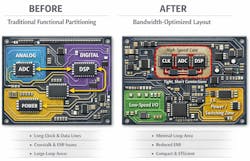
As seen in the figure, a “traditional” approach to layout can lead to long clock and data lines, crosstalk, EMI issues, and large loop areas, which could create fresh design challenges. In contrast, the bandwidth-optimized approach reduces loop area to a minimum and reduces EMI concerns while offering a layout that’s ultimately compact and efficient.
The key insight to remember is that density improves when high-speed nets stop competing with everything else for space.
How Can Replacing Wide Parallel Buses with Serial Links Help?
There’s a hidden cost of parallelism. Parallel buses feel simple: no encoding, no latency, no SerDes complexity. But from a physical standpoint, they’re expensive because many traces require spacing, length matching, and layer changes.
The other challenge is crosstalk, which worsens with trace count and the proximity of the traces to each other. Parallel buses also result in routing channels that are wide and rigid compared to serial links. At moderate data rates, designers often spend more area routing a bus than they would on the logic needed to serialize it.
In contrast, serial links trade routing complexity for silicon complexity, which is usually a relatively good deal for designers. While a SerDes pair can occupy a few square millimeters of silicon, it comes with the benefit of eliminating numerous matched traces, bus turnaround, and termination networks, and even entire routing layers.
The main advantages from a physical perspective are:
• Fewer conductors reduce electromagnetic coupling.
• Differential serial pairs tolerate tighter spacing.
• Clock embedding eliminates separate clock routing.
One possible approach is to replace a 16- or 32-bit GPIO (general-purpose input/output) bus. This isn't a single bus like I2C or SPI. Rather, it’s a flexible interface of programmable pins on a chip like a microcontroller or SoC that software can configure as inputs to read signals or outputs.
Configuring digital pins (GPIOs) to act as specific interfaces can include SPI (serial-peripheral interface) for high-speed, short-range device communication; LVDS (low-voltage differential signaling) for noise-immune, board-to-board data links; or a custom SerDes for unique high-speed needs, often converting parallel data to serial and back for efficient transmission.
It can also pay dividends for designers to use multi-drop serial links instead of star-routed parallel signals and consolidate configuration and status lines into a single control link.
However, serial doesn’t win when it comes to extremely latency-sensitive paths or with ultra-low-cost designs where SerDes silicon dominates bill of materials (BOM). They also tend to be the wrong choice for very low-speed buses with abundant board space.
But when serial works, it works. In consumer electronics, the technology can reduce layer count and enclosure size. Serial links can also dramatically improve slot density in backplanes and other modular systems. On top of that, they can be ideal for electronic systems operating in harsh conditions, since having fewer interconnects helps improve reliability and EMI robustness.
The architectural lesson is clear: one or two fast lanes often outperform multiple slow ones.
Why It Makes Sense to Move “Glue Logic” into Configurable Devices
The glue logic “trap” is simply that small logic functions, from address decoding to signal conditioning and power sequencing, accumulate over time in designs. Individually trivial, collectively they can consume a surprising amount of board area — and even more routing resources.
Consolidation improves density. That’s because a small CPLD (complex programmable logic device) or FPGA (field-programmable gate array) can replace dozens of discrete gates while eliminating point-to-point routing between them, centralizing logic near its consumers, and reducing package count and placement overhead.
From a density standpoint, routing is often the dominant cost, not silicon. Other advantages include:
• Reduced net count: Fewer external connections means tighter placement.
• Timing control: Internal routing is shorter and more predictable.
• Late-stage flexibility: Changes don’t require board rework or redesign
When consolidating glue logic into a configurable logic device or other programmable chip, it’s important to choose low-pin-count, non-BGA devices, particularly when circuit density is the goal. Other tips: Use internal pull-ups, terminations, and clocking to reduce externals and keep configuration interfaces simple and local.
There are several product-specific best practices to keep in mind:
• Industrial control: CPLDs excel at sequencing, interlocks, and legacy interfaces.
• Automotive: Consolidation improves reliability and reduces solder joints.
• Prototypes and evolving products: FPGAs absorb future changes without growth in board area.
The key tradeoff is that a modest increase in device complexity yields a large reduction in board complexity.
How Does System Architecture Sets Limits on Circuit Density?
PCB density is often treated as a layout optimization problem. In reality, though, architecture defines the upper bound. Partitioning by bandwidth, embracing serial links, and consolidating glue logic all exploit the same principle: shorter, fewer, and more purposeful connections.
Designers who adopt these strategies early put themselves in a better position to achieve smaller boards with lower layer counts, which ultimately contribute to better signal integrity and higher manufacturability.
In high-density systems, elegance begins long before routing starts.
>>Download the PDF of this article
About the Author

Alan Earls
Contributing Editor
Comment About the Article
To join the conversation, and become an exclusive member of Electronic Design, create an account today!

Leaders relevant to this article: