GaN Transistors Up the Game in Reliability and Power Efficiency
Download this article in PDF format.
Have you used gallium-nitride (GaN) transistors in your designs yet? If not, now may be the time to give it some consideration. GaN devices have been around for several years now, but improved manufacturing methods now make them less expensive than a year or so ago.
In addition, GaN devices have become more reliable, and enhanced switching specifications bring greater efficiency. If you’re designing electronic power equipment, you may be overlooking a superior solution that could bring some real improvements and benefits to your design.
Sponsored Resources:
- 20 million GaN reliability hours and counting
- GaN drives energy efficiency to the next level
- GaN: from watts to kilowatts
GaN Update
The workhorse of power electronics for the past several years has been the popular LDMOS transistor. This rugged device has undergone continual improvements and its cost has dropped. These enhancement-mode components can handle many hundreds of watts of power and switch fast enough for many types of switch-mode power supplies (SMPS). Its limitations are primarily speed, lack of ability to handle high voltages, and inefficiencies. Nevertheless, the LDMOS has found its way into many SMPS designs as well as RF power amplifiers (<2 GHz) thanks to its low cost and multiple suppliers.
However, a few years ago, multiple semiconductor vendors launched new transistors based on wide-bandgap (WBG) materials that offer higher electron mobility and bandgap energy than silicon. As a result, they can operate at much higher frequencies and switch faster than the LDMOS devices they’re replacing.
The most common WBG devices are compound semiconductors using gallium arsenide (GaAs), GaN, and silicon carbide (SiC). While they’re a bit harder to make and cost more than Si LDMOS varieties, these devices deliver some additional benefits. For example, they can also withstand much higher voltages and higher operating temperatures. And their low on-resistance and faster switching capability makes them much more efficient.
GaN devices have really made a name for themselves in the RF field. Their high-frequency capability extends to about 50 GHz and they can withstand operating voltages up to 100 V. GaN RF transistors have now been widely incorporated into many communications devices like radio transmitters, radars, satellites, and electronic-warfare equipment of all types. New GaN devices are now showing up more in power equipment.
GaN Transistors
GaN transistors split into two main categories: the high-electron-mobility transistor (HEMT) FET and the standard enhancement-mode MOSFET. HEMT FETs conduct continuously and need a negative voltage on the gate to bias them and control the drain current. HEMTs are more like MESFETs, a high-frequency JFET. They’re a bit tricky to work with as they require special gate drive and biasing. Standard enhancement-mode MOSFETs are generally easier to use, but the gate-threshold voltage varies from one device to the next. With the gate bias and control problem being solved, though, the GaN HEMT is easy to design with.
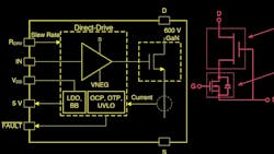
One of the newer HEMT GaN devices is Texas Instruments’ LMG341xR070. It’s a GaN power device, but it has an integrated gate driver along with multiple protection features like overcurrent protection (OCP), overtemperature protection (OTP), and undervoltage lockout (UNLV). Figure 1 shows a simplified diagram of the LMG341xR070.
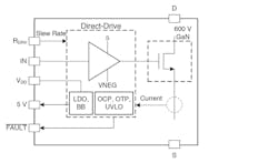
Some of its key specifications include:
- Maximum drain-source voltage: 600 V (up to 800 V for transients)
- Maximum continuous drain current: 40 A at 25°C (30 A at 100°C)
- DC supply voltage: 20 V (internal 5-V LDO is built-in to operate external circuits)
- Adjustable slew rate from 30 to 100 V/ns
- On-resistance typically 70 mΩ
- Internal circuitry generates a negative supply voltage to power the gate driver and other circuits
- Packaging: 8- × 8-mm QFN
Exceptional Competitive Features
The LMG341xR070 GaN transistors have some excellent competitive features. First, the TI devices are very reliable—the company has been testing its GaN power switches collectively for about 20 million hours. Even when used in hard-switching applications, like most SMPS, where simultaneous high-current and high-voltage transients often occur, reliability is sound.
Second, these devices are more efficient. With faster selective switching of 30 V/ns to 100V/ns and low on-resistance in the 50- to 150-mΩ range, efficiency is typically better than comparable devices. This provides the highest switching speed in the industry along with 50% lower losses in 65-W to >10-kW applications. And third, the LMG341xR070 is smaller than most other comparable devices.
The bottom line is that GaN can deliver more energy in less space, ultimately saving energy and lowering operating costs. And you don’t have to fool with the gate drive and biasing.
How GaN Devices Work
GaN HEMT devices are depletion-mode FETs. Thus, they’re conducting with zero gate voltage. To bias the transistor and control the drain current, a negative voltage is applied to the gate. This means a negative power supply and some bias voltage that typically needs to be applied in a specific turn-on sequence such as gate voltage first, drain voltage next, etc. These problems are off-putting to most designers who desire the benefits of the HEMT GaN transistors but don’t want to deal with the bias and drive complexity. The integral gate driver in the LMG341xR070 takes care of these issues.
Enhancement-mode MOSFETs are commonly used in power switching applications. These devices are normally off until gate-threshold voltage is applied. This configuration is usually easier to design with.
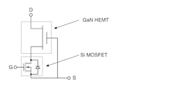
While enhancement-mode GaN transistors are now available, a popular early solution is to connect the HEMT device in cascode with an ordinary silicon enhancement-mode MOSFET (Fig. 2). This combination gives the benefits of GaN in addition to enhancement-mode operation. With the LMG341xR070, you no longer need to resort to such configurations.
In Summary
If you’re designing any of the following products or similar, your circuits can perform better with GaN devices:
- Industrial and commercial switch-mode power supplies
- Industrial motor drives
- DC-DC converters
- Regulators
- PFC circuits
- Battery chargers
- Uninterruptible power supplies (UPS)
- Solar inverters
GaN transistors still compete with other power devices such as the LDMOS and SiC MOSFETs. However, GaN devices offer some superior specifications and features that set them apart. They’re more efficient, faster, and support supply voltages to 600 V. They can handle power levels up to about 10 kW. And, as a result of 20 million hours of testing, reliability is excellent. To top it off, the integrated gate driver and all of the protection circuits make design fast and easy.
Sponsored Resources:
About the Author

Lou Frenzel
Technical Contributing Editor
Lou Frenzel is a Contributing Technology Editor for Electronic Design Magazine where he writes articles and the blog Communique and other online material on the wireless, networking, and communications sectors. Lou interviews executives and engineers, attends conferences, and researches multiple areas. Lou has been writing in some capacity for ED since 2000.
Lou has 25+ years experience in the electronics industry as an engineer and manager. He has held VP level positions with Heathkit, McGraw Hill, and has 9 years of college teaching experience. Lou holds a bachelor’s degree from the University of Houston and a master’s degree from the University of Maryland. He is author of 28 books on computer and electronic subjects and lives in Bulverde, TX with his wife Joan. His website is www.loufrenzel.com.
Comment About the Article
To join the conversation, and become an exclusive member of Electronic Design, create an account today!

Leaders relevant to this article: