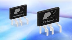
LinkSwitch-3 ICs Meet 2016 DoE 6 EPS Efficiency Regulations
Power Integrations has launched its LinkSwitch™-3 family of highly integrated monolithic switching ICs. The new devices deliver accurate primary-side regulation for chargers and adapters up to 10 W, making them suitable for smartphones, tablets and other mobile devices, particularly those subject to 30 mW no-load limitations, such as upcoming mandatory US DoE EPS efficiency regulations and EU CoC Tier 2 guidelines.
LinkSwitch-3 ICs simplify CV/CC charger designs by eliminating the need for opto-couplers and secondary-side control circuitry; a 10 W charger, for example, can be implemented using only 28 external components. The new devices provide highly accurate output voltage and current regulation, compensating for transformer and internal parameter tolerances along voltage variation from the AC line. LinkSwitch-3 ICs incorporate a 725 V power MOSFET, on/off-control state machine, high-voltage switched current source for self-biasing, frequency jittering to minimize EMI, plus cycle-by-cycle current limit and hysteretic thermal shutdown circuitry. The ICs also feature selectable cable drop compensation for improved voltage tolerance over load.
LinkSwitch-3 switcher ICs are sampling now in SO-8, eSIP-7 and eSOP-12 packages.

