Zero IQ IC Protects Against Reverse Polarity Inputs
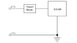
The LM74610-Q1 from Texas Instruments combines with an external NFET to configure a reverse polarity protection circuit. This configuration acts as an ideal “smart diode” that allows positive voltage inputs, but prevents negative inputs from reaching a load, as shown in Fig. 1. This basic smart diode circuit is not referenced to ground, so it has zero IQ (quiescent current). In addition, it has low reverse leakage current and low power dissipation. This solution has increased complexity compared to other approaches, but exhibits lower power dissipation that eliminates the need for heatsinks or other heat reducing methods.
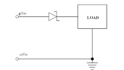
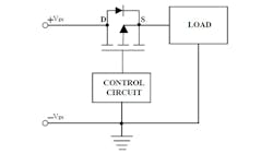
This new IC replaces two different techniques that have been employed in automotive and industrial applications requiring reverse polarity protection. One technique uses Schottky diodes (Fig. 2) and the other uses PFETs (Fig. 3), to protect the load in case a negative polarity input is received. In automotive systems this can occur due to wrong jump starts or inductive spikes.
Although Fig. 2 is a simple circuit, it has the disadvantage of high forward voltage (VF) when the diode conducts. For example, the typical VF of a Schottky diode is ~0.4V and can result in relatively high operating temperatures if conducting for a long time. Operating at 10 A, the diode power dissipation can reach 5 to 10 W, which could affect its reliability and require removal of heat to a safe level. Another disadvantage is the diode’s relatively high reverse leakage current.
PFET solutions are inefficient for high load current and low input voltage. Plus, the PFET has higher IQ and higher system cost. Using an NFET with a controller IC is a more effective and efficient substitute for the PFET in reverse polarity protection circuitry. The NFET’s lower RDS(ON) results in a lower on state forward voltage power loss than a PFET.
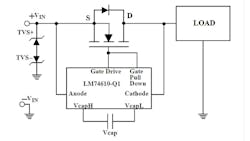
The LM74610-Q1 and an external N-channel MOSFET can replace a diode or PFET reverse polarity solution in power systems. The voltage across the MOSFET source and drain is constantly monitored by the LM74610-Q1 anode and cathode pins. An internal charge pump provides the gate drive for the external MOSFET. Forward conduction is through the MOSFET 98% of the time and through its body diode 2% of time when energy is stored in an external charge pump capacitor Vcap (Fig. 4). This stored energy is used to drive the gate of the MOSFET. The voltage drop depends on the RDS(ON) of the MOSFET. The LM74610-Q1 has no ground reference so it resembles a diode.
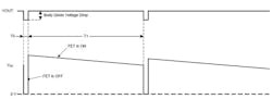
When power is initially applied, the load current (ID) flows through the MOSFET body diode and produces a voltage drop (VF) during t0, as shown in Fig. 5. This forward voltage drop across the body diode of the MOSFET is used to charge the charge pump capacitor, Vcap. During t0, the charge pump capacitor Vcap is charged to a 6.3V threshold (typical).
Once the voltage on the capacitor reaches 6.3V, the charge pump is disabled and the MOSFET turns ON. The energy stored in the capacitor is used to provide the gate drive for the MOSFET (t1 in Fig. 6). When the MOSFET is ON, it provides a low resistive path for the drain current to flow and minimizes the power dissipation associated with forward conduction. The power losses during the MOSFET ON state depend primarily on its RDS(ON) and load current. When the capacitor voltage reaches its lower threshold, VcapL, 5.15V (typical), the MOSFET gate turns OFF. The drain current, ID, will then begin to flow through the body diode of the MOSFET, causing the MOSFET body diode voltage drop to appear across the anode and cathode pins. Then, the charge pump circuitry is re-activated and begins charging Vcap.
LM74610-Q1 operation keeps the MOSFET ON approximately 98% duty cycle (typical) regardless of the external charge pump capacitor value. This is the key factor to minimizing the power losses. The forward voltage drop during this time is limited by the MOSFET’s RDS(ON).
Once the MOSFET is turned ON, the Anode and Cathode pins constantly sense the voltage difference across the MOSFET to determine the magnitude and polarity of the voltage across it. When the MOSFET is on, the voltage difference across Anode and Cathode pins depends on the RDS(ON) and load current. If the voltage difference across source and drain of the external MOSFET becomes negative, it is sensed as a fault condition by Anode and Cathode pins and gate is turned off by Gate Pull Down pin (Fig. 4). The consistent sensing of voltage polarity across the MOSFET enables the LM74610-Q1 to provide a fast response to the power source failure and limit the amount and duration of the reverse current flow.
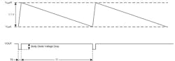
VcapH and VcapL are high and low voltage thresholds respectively that the LM74610-Q1 uses to detect when to turn the charge pump circuitry ON and OFF. The capacitor charging and discharging time can be correlated to the duty cycle of the MOSFET gate. Figure 6 shows the voltage behavior across Vcap. During the time period t0, the capacitor is storing energy from the charge pump. The MOSFET is turned off and current flow is only through the body diode during. The conduction though the MOSFET’s body diode is for a short time (2% typical), which rules out the chances of overheating the MOSFET, regardless of the output current. Once the capacitor voltage reaches its high threshold, the MOSFET turns off and charge pump circuity is deactivated until the Vcap reaches its low voltage threshold at t1.
Place a ceramic capacitor between VcapL and VcapH. A capacitor value of 220nF to 4.7uF with X7R/COG characteristic and 16V rating or higher is recommended for this application. A higher value capacitor sets longer MOSFET ON time and OFF time; however, the duty cycle remains at ~98% for MOSFET ON time irrespective of capacitor value.
Important parameters in the selection of the external MOSFET are:
- Maximum continuous Drain current ID (must exceed the maximum continuous load current)
- Maximum drain-to-source voltage VDS(MAX) (must be high enough to withstand the highest differential voltage seen in the application)
- Gate-to-source threshold voltage VGS(TH) (≤3V)
- Drain-to-source On resistance RDS(ON)
Although there are no positive VDS limitations, it is recommended to use MOSFETS with voltage rating up to 45V for automotive applications, since the LM74610-Q1 has a reverse voltage limit of -45V.
Features of LM74610-Q1 include:
- QEC-Q100 qualified
- Exceeds HBM ESD Classification Level 2
- Device CDM ESD Classification Level C4B
- Meets CISPR EMI specification
- Meets automotive ISO7637 transient requirements with suitable external TVS
- 45 V maximum reverse voltage
- Charge pump gate driver for external NFET
- Low reverse leakage current
- Zero IQ
- 2 µs response to reverse polarity
- -40°C to 125°C operating ambient temperature
About the Author

Sam Davis
Sam Davis was the editor-in-chief of Power Electronics Technology magazine and website that is now part of Electronic Design. He has 18 years experience in electronic engineering design and management, six years in public relations and 25 years as a trade press editor. He holds a BSEE from Case-Western Reserve University, and did graduate work at the same school and UCLA. Sam was the editor for PCIM, the predecessor to Power Electronics Technology, from 1984 to 2004. His engineering experience includes circuit and system design for Litton Systems, Bunker-Ramo, Rocketdyne, and Clevite Corporation.. Design tasks included analog circuits, display systems, power supplies, underwater ordnance systems, and test systems. He also served as a program manager for a Litton Systems Navy program.
Sam is the author of Computer Data Displays, a book published by Prentice-Hall in the U.S. and Japan in 1969. He is also a recipient of the Jesse Neal Award for trade press editorial excellence, and has one patent for naval ship construction that simplifies electronic system integration.
You can also check out his Power Electronics blog.
Comment About the Article
To join the conversation, and become an exclusive member of Electronic Design, create an account today!

Leaders relevant to this article: