Digital Compensation Simplifies Design, Improves Performance Of Point-of-Load Module
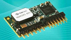
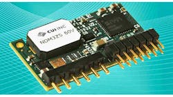
CUI’s recently introduced NDM3ZS-60 dc-dc point of load module uses Intersil’s newest digital controller IC, the ZL8800, which incorporates a range of advanced digital features. Its ChargeMode™ Control technology enhances the supply’s transient response performance by responding to a transient load step in a single switching cycle. With an innovative new digital control scheme, the need for compensation is completely removed, keeping the system stable on a continuous basis. This feature enables designers to bypass the traditional practice of building-in margins to account for factors such as component aging, manufacturing variations, and temperature, which inevitably lead to higher component cost and longer design cycles. The NDM3ZS’s constant compensation feature allows the module to maintain optimum stability in real time as conditions change.
Related Articles
- Auto Compensation Enhances Power Supply Designs
- Self- Compensating Digital Point-of-Load Modules
- Adaptive On-Time DC-DC Converters Combine Speed and Efficiency
- Controller IC Employs Real-Time Adaptive Loop Compensation, PMBus
- Adaptive On-Time DC-DC Converters Combine Speed and Efficiency
This series is also the first non-isolated design to incorporate CUI’s patented Solus® Power Topology that integrates a conventional buck converter into a SEPIC converter to form a SEPIC-fed buck converter. The result is a single stage topology with one magnetic element, one control switch and two commutation switches that are optimally controlled by pulse-width modulation (PWM). The Solus Topology increases total efficiency by distributing the energy delivery into multiple paths, reducing circuit conduction losses by nearly 50%.
The SEPIC-fed buck converter (see Fig. 1.) addresses two critical issues: efficiency and transient response. A buck converter is integrated into a SEPIC to receive energy from the SEPIC inductors and the outputs of both deliver energy to the load in parallel. When the controlling switch – shared by both converters – is ON, the buck portion delivers energy to the load while the SEPIC portion stores energy in the magnetic element and feeds the buck portion. When the controlling switch is OFF, the stored energy is delivered to the load through both the buck and the SEPIC portions. The new converter combines the characteristics of both buck and SEPIC converters, resulting in reduced voltage and current levels in the magnetic and switching devices and leading to reduced conduction and switching losses.
Additionally, an inherent gate-charge-extraction mechanism facilitates extremely fast turn-off of the control switch, essentially eliminating its turn-off loss. Furthermore, a new volt-second structure on the magnetic element significantly improves transient response of the power stage. Compared to a conventional buck converter, the lower voltage and current stresses coupled with an inherent gate charge extraction (GCE) process reduces switching turn-on losses by 75% and switching turn-off losses by 99% on the control FET.
CUI’s SEPIC-fed buck topology allows the NDM3ZS-60 to hit impressive performance metrics. Efficiency peaks at 91.3% at 12Vdc in to 1.0Vdc out, 50% load. Efficiency remains high up to full load at 88.5%. Transient response is also greatly improved with the SEPIC-fed buck. At 12 Vdc in to 1 Vdc out with a 30 A load step (from 15 A to 45 A) and a 10 A/µs slew rate, peak voltage is 16 mV with typical external capacitance required.
The NDM3ZS-60 series is available with an input range of 7.2~14 Vdc and a programmable output range of 0.6~1.5 Vdc. Additional features include voltage sequencing, voltage tracking, synchronization and phase spreading, programmable soft start and stop, as well as a host of monitoring capabilities. All features are dynamically programmable via PMBus commands or through CUI’s Novum ACE™ GUI.
The family is available in three compact configurations, a through-hole vertical version measuring 33.02 (L) X 8.92 (W) X 18.11 (H) mm and a horizontal version measuring 33.02 x 18.11 x 7.44 mm that is offered in surface mount or through-hole configurations. For added flexibility during the development process, the modules are footprint nested to accommodate dual layout needs in the event that design requirements change. Additionally, the NDMZ3S-60 is footprint compatible with 40 A and 50 A digital modules currently available from several manufacturers. This provides up to a 50% increase in power density over existing solutions.
ZL8800
The ZL8800 used in the NDM3ZS-60 is a dual output or dual phase digital DC-DC controller. The controller utilizes Intersil’s proprietary ChargeMode™ to deliver fast transient without the need for compensation. Each output can operate independently or be used together in a multiphase configuration for higher current applications.
This controller IC features cycle-by-cycle output overcurrent protection. Input voltage, output voltages and DrMOS/MOSFET driver supply voltages are undervoltage and overvoltage protected. Two external and one internal temperature sensor are available for temperature monitoring, one of which is used for under and over-temperature protection.
With full PMBus™ compliance, the ZL8800 is capable of measuring and reporting input voltage, input current, output voltage, output current as well as the device’s internal temperature, two external temperatures and an auxiliary voltage input.
Prior to introduction of the NDM3ZS-60, CUI introduced two families of digital point of load dc-dc supplies that have auto compensation: NDM2Z and NDM2P. The NDM2Z design uses the Intersil/Zilker ZL8101M regulator IC whereas the NDM2P uses the Powervation PV3012 control IC.
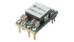
The 50A NDM2Z (Fig. 2) and NDM2P supplies deliver 91% efficiency with 12 Vdc input and 1.0 Vdc output at 50% load. Both are available in three compact DIP configurations, a 12 A version is 0.827 x 0.500 X 0.284 in., a 25 A version is 1.01 x 0.54 x 0.284 in., and a 50 A version is 1.215 x 0.79 x 0.36 in. Both supplies have a 4.5~14 Vdc input range and a programmable output range of 0.6~5.0 Vdc in the 12A version and 0.6~3.3 Vdc in the 25 A and 50 A versions. Other features include active current sharing, voltage sequencing, voltage tracking, synchronization and phase spreading, programmable soft start and stop, as well as a host of monitoring capabilities. All features are dynamically programmable via PMBus commands or through CUI’s GUI.
The NMD2Z uses an Intersil ZL8101, a digital synchronous buck controller with a constant frequency pulse width modulator (PWM). It utilzes external drivers to allow for flexibility in power level with external power MOSFETs, capacitors, and inductors (Fig. 3). Integrated sub-regulation circuitry allows single supply operation of 4.5V to 14 V, without needing a secondary bias supply.
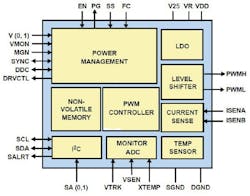
The ZL8101’s auto compensation measures the characteristics of the power train and determines the required compensation providing a setting optimizing transient response. Its digital PWM loop interfaces with external drivers. The ZL1505 is the recommended driver for the ZL8101, but it can also work with other drivers whose inputs range between 2.5V and 5.5V or with DrMOS devices. The ZL1505’s PWMH and PWML inputs connect to similar-marked pins on the ZL8101outputs.
Select each of the external synchronous output power MOSFETs primarily on their RDS(ON) and secondarily on total gate charge. The actual power converter’s output current depends on the characteristics of the drivers and output MOSFETs.
You can configure an extensive set of power management functions using simple pin connections or standard PMBus commands using the I2C/SMBus interface. Once enabled, the ZL8101 is immediately ready to regulate power and perform power management tasks with no programming required. Advanced configuration options and real-time configuration changes are available via the I2C/SMBus interface, if desired, and continuous monitoring of multiple operating parameters is possible with minimal interaction from a host processor. An on-chip non-volatile memory (NVM) saves configuration data.
Powervation PV3012
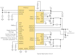
Powervation’s PV3012 auto compensation IC used in CUI’s NDM2P is a single output, dual or single-phase digital synchronous buck controller for point-of-load (POL) applications (Fig. 4). This allows the IC to dynamically control the output voltage, slew rates, power states, as well as monitor the voltage regulator for telemetry purposes via PMBus.
You can configure the PV3012’s operating parameters through I2C communication, external resistors, or programming stored in its non-volatile memory (NVM). The PV3012 includes a Digital Signal Processor (DSP), RISC Processor and precision data acquisition system. Its dual-core architecture yields a voltage regulator for applications that require flexibility for loads that may change over a supply’s lifetime.
To implement closed loop compensation the PV3012 uses a discrete-time adaptive control algorithm updated in real-time, on a switching cycle-by-cycle basis, running on the DSP core. This eliminates external compensation components or the need to manually retune the compensation should the characteristics of the load change (i.e., load capacitance, inductances, etc.). Optimized for high performance with low power consumption, the DSP core’s adaptive algorithm is independent of general housekeeping, fault management and configuration tasks.
A low-latency precision analog-digital converter (ADC) samples and quantizes voltages, currents, and temperatures. This information is used as inputs for proprietary algorithms that the DSP and RISC processors compute, and then use to determine optimal PWM switching behavior, fault management, etc. Architecture for digital power management solutions is a multi-processor system-on-chip (SoC) with an ultra-lean proprietary dual core DSP and RISC processors. The SoC contains RAM and NVM, power conversion blocks, SMBus serial interface, ADCs and DACs (digital-to-analog converter), and oscillator and phase lock loop timing sources.
Figures
Fig. 1. The NDM3ZS-60’s SEPIC-fed Buck Topology allows higher power density, higher efficiency, faster transient response, and lower EMI.
Fig. 2. CUI’s NDM2Z power supply employs auto compensation that allows it to dynamically set optimum stability and transient response.
Fig. 3. Intersil’s ZL8101 IC diagram shows the PWM outputs (PWMH and PWML) that interface with an external driver like the ZL1505.
Fig. 4. Operation’s PV3012 IC is real-time auto compensation IC with a single output, dual or single phase digital synchronous buck controller for POL applications
About the Author

Sam Davis
Sam Davis was the editor-in-chief of Power Electronics Technology magazine and website that is now part of Electronic Design. He has 18 years experience in electronic engineering design and management, six years in public relations and 25 years as a trade press editor. He holds a BSEE from Case-Western Reserve University, and did graduate work at the same school and UCLA. Sam was the editor for PCIM, the predecessor to Power Electronics Technology, from 1984 to 2004. His engineering experience includes circuit and system design for Litton Systems, Bunker-Ramo, Rocketdyne, and Clevite Corporation.. Design tasks included analog circuits, display systems, power supplies, underwater ordnance systems, and test systems. He also served as a program manager for a Litton Systems Navy program.
Sam is the author of Computer Data Displays, a book published by Prentice-Hall in the U.S. and Japan in 1969. He is also a recipient of the Jesse Neal Award for trade press editorial excellence, and has one patent for naval ship construction that simplifies electronic system integration.
You can also check out his Power Electronics blog.
Comment About the Article
To join the conversation, and become an exclusive member of Electronic Design, create an account today!

Leaders relevant to this article: