Two-Phase, Synchronous Boost Regulator IC Delivers Up to 15 V
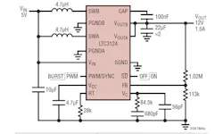
One of the latest Linear Technology dc-to-dc converter ICs is the LTC3124, whose application circuit is shown in Fig. 1.
The regulator employs an external resistive voltage divider from VOUT to FB to SGND to program the output from 2.5 V to 15 V. When set for a 12 V output, it can deliver up to 1.5 A continuously from a 5 V input. Its 2.5 A per phase current limit, along with the ability to program output voltages up to 15 V, make the IC suitable for a variety of applications.
The use of two phases equally spaced 180° apart, doubles output ripple frequency, and significantly reduces output capacitor ripple current. Although this architecture requires two inductors, rather than a single inductor, it has several important advantages:
• Substantially lower peak inductor current allows the use of smaller, lower cost inductors.
• Significantly reduced output ripple current minimizes output capacitance requirement.
• Higher frequency output ripple is easier to filter for low noise applications.
• Input ripple current is also reduced for lower noise on VIN.
With two-phase operation, one phase always delivers current to the load whenever VIN is greater than one-half VOUT (for duty cycles less than 50%). As the duty cycle decreases further, load current delivery between the two phases begin to overlap, occurring simultaneously for a growing portion of each phase as the duty cycle approaches zero. Compared with a single-phase converter this significantly reduces both the output ripple current and the peak current in each inductor.
The LTC3124 provides an advantage for battery-powered systems, it can start up from inputs as low as 1.8 V and continue to operate from inputs as low as 0.5 V, while producing output voltages greater than 2.5 V. This extends operating times by maximizing the amount of energy extracted from the input source. The limiting factors for the application are the ability of the power source to supply sufficient power to the output at the low input voltage, and the maximum duty cycle, which is clamped at 94%. At low input voltages, small voltage drops due to series resistance become critical and limit the converter’s power delivery.
Even if the input voltage exceeds the output voltage, the IC will regulate the output, enabling compatibility with any battery chemistry. The LTC3124 is an ideal solution for boost applications requiring outputs up to 15 V where high efficiency, small size and high reliability are defining factors.
Soft-Start
Internal soft-start limits the LTC3124’s inrush current during start-up while minimizing external components. Soft-start utilizes a linearly increasing ramp of an error amplifier reference voltage from zero to its nominal value of 1.2 V in approximately 10 ms, with the internal control loop driving VOUT from zero to its final programmed value. This limits the inrush current drawn from the input source. As a result, the duration of the soft-start is largely unaffected by the size of the output capacitor or the output regulation voltage. The closed-loop nature of soft-start allows the converter to respond to load transients that might occur during the soft-start interval.
You can program the switching frequency from 100 kHz to 3 MHz and synchronize it with an external clock. A resistor from the RT pin to ground (Fig. 1) sets the switching frequency.
For applications demanding the lowest possible noise operation, set the PWM/SYNC pin (Fig. 1) high to operate in a continuous frequency mode. At all current levels this mode minimizes possible interference of switching noise with noise-sensitive circuitry, slightly reducing light load efficiency. Connecting an external clock to this pin synchronizes it with the internal oscillator and disables Burst Mode operation. A clock pulse width of 100 ns, minimum, is required to synchronize the oscillator. For proper operation the external RT resistor must set the switching frequency slightly below the desired synchronization frequency.
Holding the PWM/SYNC pin low activates the Burst Mode. This mode improves efficiency at light loads and reduces standby current at no load. Output current (IOUT) capability in Burst Mode operation is significantly less than in PWM mode and varies with VIN and VOUT. The logic input thresholds for this pin are determined relative to VCC with a low being less than 10% of VCC and a high being greater than 90% of VCC. The LTC3124 will operate in fixed frequency PWM mode even if Burst Mode operation is commanded during soft-start.
In Burst Mode operation, only Phase A of the LTC3124 is operational, while Phase B is disabled. Phase A inductor current is initially charged to approximately 700 mA by turning on the N-channel MOSFET switch, at which point the N-channel switch is turned off and the P-channel synchronous switch is turned on, delivering current to the output. When the inductor current discharges to approximately zero, the cycle repeats. In Burst Mode, energy is delivered to the output until the nominal regulation value is reached, then the LTC3124 transitions into a very low quiescent current sleep state. In sleep, the output switches are turned off and the LTC3124 consumes only 25 μA of quiescent current. When the output voltage drops approximately 1%, switching resumes. This maximizes efficiency at very light loads by minimizing switching and quiescent losses. Output voltage ripple in Burst Mode operation is typically 1% to 2% peak-to-peak. Additional output capacitance (22 μF or greater), or the addition of a small feedforward capacitor (10 pF to 50 pF) connected between VOUT and FB can help further reduce the output ripple.
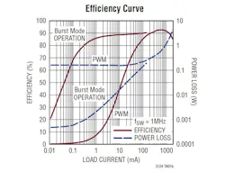
Fig. 2 compares the performance of the LTC3124 in the PWM and Burst Mode for the circuit in Fig. 1.
Output Disconnect
An output disconnect feature allows the output to be completely discharged in shutdown. It also limits the inrush of current during start-up, minimizing surge currents seen by the input supply. This allows output short-circuit protection while maintaining a maximum set current limit. To reduce power dissipation under overload and short-circuit conditions, the peak switch current limits are reduced to approximately 2 A. Once VOUT exceeds approximately 1.5 V, the current limits are reset to their nominal values of 3.5 A per phase.
Output disconnect eliminates body diode conduction of the internal P-channel MOSFET synchronous rectifiers. It also allows VOUT to discharge to 0V during shutdown, and draw no current from the input source. To obtain the advantages of output disconnect, do not use an external Schottky diode connected between SWA, SWB (Fig. 1) and VOUT. The output disconnect feature also allows VOUT to be pulled high, without backfeeding the power source connected to VIN.
RDS(ON) of the internal N-channel MOSFET switches is only 130 mΩ and the associated P-channel switches are 200 mΩ. With its low RDS(ON) and low gate charge internal N-channel MOSFET switches and P-channel MOSFET synchronous rectifiers, the LTC3124 achieves high efficiency over a wide range of load current. Its internal 2.5 A per phase switches together can deliver 5 A of switch current. These 18 V switches can deliver output voltages as high as 15 V from an input voltage range of 1.8 V at start-up (0.5 V when running) to 5.5 V, making it ideal for battery-powered systems.
Current limit comparators shut off the N-channel MOSFET switches once their respective peak current is reached. Peak switch current per phase is limited to 3.5 A, independent of input or output voltage, unless VOUT is below approximately 1.5 V, resulting in the current limit being approximately half of the nominal peak values.
Lossless current sensing converts the peak current signals of the N-channel MOSFET switches into voltages that are summed with their respective internal slope compensation. The summed signals are compared to the error amplifier outputs to provide a peak current control command for the PWMs.
The LTC3124 uses current mode control, with internal adaptive slope compensation. Current mode control eliminates the second order filter due to the inductor and output capacitor exhibited in voltage mode control, and simplifies the power loop to a single pole filter response. Because of this fast current control loop, the power stage of the IC combined with the external inductor can be modeled by a transconductance amplifier and a current controlled current source.
The current mode zero is a right-half plane (RHP) zero that can be an issue in feedback control design, but is manageable with proper external component selection. Also, note that the RHP zero is a minimum at minimum input voltage and maximum output current for a given output voltage. As a general rule, the crossover frequency should be set to less than one-sixth of the RHP zero, and under one-eighth of the switching frequency. Once you select the crossover frequency you can calculate the compensation component values.
Additional features include output overvoltage protection, and robust short-circuit protection. If the die temperature exceeds 170°C typical, the LTC3124 will go into thermal shutdown (TSD). All switches will be shut off until the die temperature drops by approximately 7°C, when the device re-initiates a soft-start and switching is re-enabled.
The SD (insert overscore) pin (Fig. 1) is a logic controlled shutdown input. Pulling this pin above 1.6 V enables normal, free-running operation. Forcing this pin below 0.25 V shuts the LTC3124 off, with quiescent current below 1 μA. SD (insert overscore) can be driven above VIN or VOUT, as long as it is limited to less than its absolute maximum rating.
There are four versions of this family. LTC3124EDHC and LTC3124EFE are both available in 16-lead 3 mm x 5 mm DFN and thermally enhanced TSSOP packages, respectively. Industrial grade versions, the LTC3124IDHC and LTC3124IFE, are guaranteed to operate over the –40 °C to 125 °C operating junction temperature range and a high temperature grade version, the LTC3124HFE is guaranteed to operate over –40 °C to 150 °C. The combination of its thermally enhanced 3 mm x 5 mm DFN-16 (or TSSOP-16) package providing the compact footprint required in battery-powered, handheld applications.
About the Author

Sam Davis
Sam Davis was the editor-in-chief of Power Electronics Technology magazine and website that is now part of Electronic Design. He has 18 years experience in electronic engineering design and management, six years in public relations and 25 years as a trade press editor. He holds a BSEE from Case-Western Reserve University, and did graduate work at the same school and UCLA. Sam was the editor for PCIM, the predecessor to Power Electronics Technology, from 1984 to 2004. His engineering experience includes circuit and system design for Litton Systems, Bunker-Ramo, Rocketdyne, and Clevite Corporation.. Design tasks included analog circuits, display systems, power supplies, underwater ordnance systems, and test systems. He also served as a program manager for a Litton Systems Navy program.
Sam is the author of Computer Data Displays, a book published by Prentice-Hall in the U.S. and Japan in 1969. He is also a recipient of the Jesse Neal Award for trade press editorial excellence, and has one patent for naval ship construction that simplifies electronic system integration.
You can also check out his Power Electronics blog.
Voice Your Opinion!
To join the conversation, and become an exclusive member of Electronic Design, create an account today!

Leaders relevant to this article:


