2 A Synchronous Buck DC-DC Converter Supports Automotive Applications
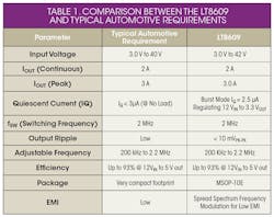
With its 3.0 V to 42 V input range, the LT8609 is ideal for automotive applications that must regulate through cold-crank, load dump transients, and stop-start driving. The IC maintains a minimum dropout of 200 mV (at1A) under all conditions, enabling it to excel in automotive cold-crank situations (see sidebar: Cold Crank And Load Dump). Spread spectrum frequency modulation and special design techniques offer low-EMI operation to minimize noise in automotive and industrial environments. The LT8609’s characteristics mirror those required by a switch-mode buck converter intended for the automotive environment, as shown in Table 1.
Related Articles
- Auto Compensation Voltage Regulator ICs Enhance Power Supply Designs
- Synchronous Buck Converter Delivers 12A with Ultra-Fast Load Step Response
- Innovative Design Shrinks Buck Converter Size, Cuts External Parts Count
- Digital Control Squeezes 40 A from Buck Converter
- Buck-Converter Design Demystified
- The eGaN® FETShootout Volume 7: Buck Converters
You can set the switching frequency between 200 kHz and 2.2 MHz using an external resistor. Selecting a switching frequency is a trade-off between efficiency, component size, and output step-down ratio. The advantage of high frequency operation is that smaller inductor and capacitor values may be used. The disadvantages are lower efficiency and a smaller input voltage range.
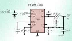
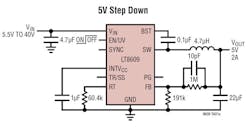
Fig. 1 shows a typical LT8609 application. In operation, the IC utilizes internal top and bottom high efficiency power switches with the necessary boost diode, oscillator, control and logic circuitry integrated into a single die. Unique design techniques and a new high speed process enable high efficiency over a wide input voltage range, and a current-mode topology enables fast transient response and excellent loop stability. Other features include internal compensation, a power good flag (PG), output soft start/tracking (TR/SS) and thermal protection.
To enhance efficiency at light loads, the LT8609 enters into a low ripple Burst Mode, which keeps the output capacitor charged to the desired output voltage while minimizing the input quiescent current and minimizing output voltage ripple. In Burst Mode the LT8609 delivers single small pulses of current to the output capacitor followed by sleep periods where the output power is supplied by the output capacitor. While in sleep mode the LT8609 draws 1.7 µA.
As the output load decreases, the frequency of single current pulses decreases and the percentage of time that the LT8609 is in sleep mode increases, resulting in much higher light load efficiency than most converters. By maximizing the time between pulses, a typical application with no output load exhibits a quiescent current that approaches 2.5 μA.
For some applications it is desirable for the LT8609 to operate in pulse-skipping mode, which differs from the Burst Mode. In pulse-skipping, the clock stays awake at all times and all switching cycles are aligned to the clock. In this mode much of the internal circuitry is awake at all times, increasing quiescent current to several hundred μA. Also, the full switching frequency is reached at lower output load than in the Burst Mode. To enable the pulse-skipping mode you float the SYNC pin. To achieve spread spectrum modulation with pulse-skipping mode, you tie the SYNC pin high.
Applying a clock to the IC’s SYNC pin will synchronize it to an external clock frequency and operate in pulse-skipping mode. While in pulse-skipping mode its oscillator operates continuously and positive switch transitions align to the clock.
The output voltage is programmed with a resistor divider between the output and the FB pin, as shown in Fig. 1. Choose the resistor values according to:
In Fig. 1, R1 and R2 connect to the FB pin; R1 is 1MΩ and R2 is 191 kΩ. To maintain output voltage accuracy, both should be 1% resistors. The total resistance of the FB resistor divider should be as large as possible for good low light efficiency. The resistor divider presents a small load on the output, which should be minimized to optimize the quiescent current at light loads. When using large FB resistors, connect a 10pF phase lead capacitor from VOUT to FB, as shown in Fig. 1.
Component Selection
Choose the LT8609 inductor based on the application’s output load requirements. During overload or short circuit conditions the LT8609 safely tolerates operation with a saturated inductor through the use of a high-speed peak current mode architecture.
To avoid overheating and poor efficiency, choose an inductor whose RMS current rating is greater than the application’s maximum expected output load. In addition, the inductor’s saturation current (ISAT) rating should be higher than the load current plus 1/2 of the inductor ripple current.
Buck regulators draw current from the input supply in pulses with very fast rise and fall times. This requires an input capacitor to reduce the resulting voltage ripple and force this high frequency switching current into a tight local loop that minimizes EMI. Therefore, bypass the LT8609 input circuit with a A 4.7μF to 10μF, X7R or X5R ceramic capacitor.
When using a lower switching frequency use a larger input capacitance. If the input power source has high impedance, or there is significant inductance due to long wires or cables, add additional bulk capacitance using an electrolytic capacitor.
One of the output capacitor functions, along with the inductor, is to filter the square wave produced by the LT8609 that supplies the DC output. This determines the output ripple, so low impedance at the switching frequency is important. A second function is to store energy in order to satisfy transient loads and stabilize the LT8609’s control loop. Ceramic capacitors have very low equivalent series resistance (ESR) and provide the best ripple performance.
MSOP
A 10-lead thermally enhanced MSOP package provides a compact, thermally efficient footprint. There are three versions that differ only in their operating junction temperature range. The LT8609EMSE is guaranteed to meet performance specifications from 0 °C to 125 °C range with specifications over the –40 C to 125 °C are assured by design, characterization, and correlation with statistical process controls. The LT8609IMSE is guaranteed over the full –40 °C to 125 °C range, whereas the LT8609H is guaranteed over the full –40 °C to 150 °C range.
Solder the exposed pad on the bottom of the package to a ground plane. To spread the power dissipated by the LT8609 use thermal vias to tie the ground to available copper layers. If the ambient temperature approaches the maximum junction temperature rating, derate the maximum load current. Exceeding the LT8609’safe junction temperature will cause it to stop switching and indicate a fault.
By definition, all Linear Technology parts can be qualified to AEC-Q100, which requires actual testing and data logging per AEC-Q100 requirements. Because the IC was just released, AEC-Q100 testing is pending.
*************************SIDEBAR******************************
Cold Crank and Load Dump
Cold crank refers to the battery power output used to start a cold engine, which depends on the temperature of the vehicle and the battery. Two factors affect the battery output: a cold engine loads the battery more during starting and a cold car battery is less efficient. Both factors cause the battery output voltage to drop.
In automotive electronics, load dump refers to the disconnection of a vehicle battery from its associated alternator while the battery is being charged. This can cause loads connected to the alternator to see a power line surge. The peak voltage of this surge may reach 40 V and take several hundred milliseconds to decay.
About the Author

Sam Davis
Sam Davis was the editor-in-chief of Power Electronics Technology magazine and website that is now part of Electronic Design. He has 18 years experience in electronic engineering design and management, six years in public relations and 25 years as a trade press editor. He holds a BSEE from Case-Western Reserve University, and did graduate work at the same school and UCLA. Sam was the editor for PCIM, the predecessor to Power Electronics Technology, from 1984 to 2004. His engineering experience includes circuit and system design for Litton Systems, Bunker-Ramo, Rocketdyne, and Clevite Corporation.. Design tasks included analog circuits, display systems, power supplies, underwater ordnance systems, and test systems. He also served as a program manager for a Litton Systems Navy program.
Sam is the author of Computer Data Displays, a book published by Prentice-Hall in the U.S. and Japan in 1969. He is also a recipient of the Jesse Neal Award for trade press editorial excellence, and has one patent for naval ship construction that simplifies electronic system integration.
You can also check out his Power Electronics blog.
Voice Your Opinion!
To join the conversation, and become an exclusive member of Electronic Design, create an account today!

Leaders relevant to this article:


