42-V, 5-A Synchronous Step-Down “Silent Switcher” Limits EMI Radiation
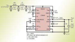
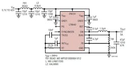
The LT8640 from Linear Technology is a monolithic, constant frequency, current mode, 5 A synchronous step-down DC/DC converter. Packaged in a 3 mm × 4 mm QFN, with integrated power switches and all necessary circuits it requires only a minimal PCB footprint. Its 2.5 μA quiescent current, with the output in full regulation, enables applications requiring high efficiency at low load currents. And, output voltage ripple is below 10 mVP-P at any load, from zero to full current. In addition, the LT8640 meets the radiated emissions specified by CISPR (international committee on radio interference) for the maximum permissible disturbance of radio receivers in the 150 kHz to 1000 MHz range. Fig. 1 shows an LT8640 circuit that provides 5 V at 5 A.
Related Articles
- Step-Down DC/DC Converter Delivers 96% Efficiency
- 2 A Synchronous Step-Down DC/DC Converter Is 93% Efficient at 2 MHz
- Step-Down DC/DC Converter Is Rated 3.5 A At 42 V
- 3 A Step-Down DC-DC Converter Boosts Energy Efficiency
- 42V, 2.5A (IOUT) & 5A (IOUT), 2MHz Step-Down DC/DC Converters
- 42V, 750mA (IOUT), 2.2MHz Step-Down DC/DC Converter
The regulator’s 42 V absolute maximum input voltage rating is important for automotive and industrial environments. Just as important, especially in automotive situations, is its dropout voltage. Often, critical 3.3 V logic supplies must be supported through cold crank situations. The LT8640 regulator maintains the close to ideal behavior in this case. Instead of higher undervoltage lockout voltages and maximum duty cycle clamps of alternative parts, the LT8640 operates down to 3.4 V inputs.
You can program the output voltage with a resistor divider between the output and the FB pin, as shown in Fig. 1. Choose the resistor values according to:
Or
When using large FB resistors, you should connect a 4.7 pF to 22 pF phase-lead capacitor from VOUT to FB.
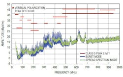
In the past, the argument against switch-mode DC/DC converters was that they can generate EMI that affects neighboring circuits. Now, the LT8640 is a “Silent Switcher” that conforms to the requirements of CISPR 25 Class 5. Fig. 2 shows the LT8640’s radiated EMI performance along with CISPR25’s radiated emission test with Class 5 peak limits. The LT8640 can run either below the AM band for even lower EMI, or above the AM band. In a setup with a 700 kHz switching frequency, the LT8640 does not exceed the noise floor in a CISPR25, Class 5 measurement.
Typically, one solution to EMI issues was to use a shielding box over the complete circuit. However, this adds significant cost in required board space, components and assembly. Moreover, adding shielding complicates thermal management and testing. Yet another way to reduce EMI is to slow down the converter’s switching edges, but this also reduces efficiency, increases minimum on- and off-times and the associated dead times; it also compromises the potential current control loop speed.
As a measure of its effectiveness, the LT8640 reduces EMI emissions by more than 25 dB compared with current state-of-the-art switching regulators. In addition, it lowers EMI by 20x in the frequency range above 30 MHz without compromising minimum on- and off-times or efficiency in an equivalent board area. It accomplishes this with no additional components or shielding, which is a significant breakthrough in switching regulator design.
The LT8640 uses a constant frequency PWM architecture and uses a resistor from the RT pin to ground to set switching frequency from 200 kHz to 3 MHz. It can be synchronized to an external frequency operating from 200 kHz to 3 MHz. AC switching losses are low, so it can be operated at high switching frequencies with minimal efficiency loss. In EMI-sensitive applications, such as those commonly found in many automotive environments; the LT8640 maintains a good EMI-efficiency balance.
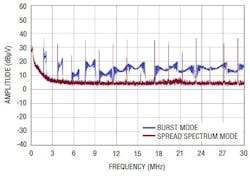
To aid EMI reduction, the LT8640 can operate in spread spectrum mode. This reduces the converter’s EMI by spreading the switching frequency energy in a narrow band over a wider band in a controlled manner. As a result, it reduces the peak spectral amplitude of the fundamental and the harmonics and lowers the radiated emission from the switching source. With spread spectrum in operation, the LT8640 varies its clock with a triangular frequency modulation of +20%. For example, with the LT8640 is programmed to switch at 2 MHz, spread spectrum mode modulates the oscillator between 2 MHz and 2.4 MHz. Fig. 3 compares amplitude vs. frequency characteristics for the Burst mode and the spread spectrum node in the LT8640.
To enhance efficiency at light loads, the LT8640 operates in low ripple Burst Mode, which keeps the output capacitor charged to the desired output voltage while minimizing the input quiescent current and minimizing output voltage ripple. In Burst Mode operation the LT8640 delivers single small pulses of current to the output capacitor followed by sleep periods where the output power is supplied by the output capacitor. Between bursts in the Burst mode, all circuits associated with controlling the output switch are shut down, reducing the input supply current to 1.7 µA. In a typical application, the input supply consumes 2.5 µA when regulating with no load.
For some applications it is desirable for the LT8640 to operate in pulse-skipping mode, offering two major differences from Burst Mode operation. First, the clock stays awake at all times and all switching cycles are aligned to the clock. In this mode most of the internal circuits are awake at all times, increasing quiescent current to several hundred μA. Second, the full switching frequency is reached at lower output load than in Burst Mode operation.
The SYNC/MODE pin selects between Burst Mode, pulse-skipping, or spread spectrum mode, and also allows synchronization to an external clock. You can tie the SYNC/MODE pin high for pulse-skipping mode with spread spectrum modulation.
You can program the output voltage ramp rate by means of the TR/SS pin. Putting an external capacitor on TR/SS enables soft starting the output to prevent current surge on the input supply. During the soft-start ramp the output voltage will proportionally track the TR/SS pin voltage.
You can set an accurate enable threshold using the EN/UV pin. If the EN/UV pin is low, the LT8640 is shut down and draws 1 µA from the input. When the EN/UV pin is above 1 V, the switching regulator becomes active.
When the LT8640’s output voltage is within the ±8% window of the regulation point, the output voltage is considered good and the open-drain PG pin becomes a high impedance and is typically pulled high with an external resistor. Otherwise, the internal pull-down device will pull the PG pin low. To prevent glitches, both the upper and lower thresholds have 0.2% hysteresis.
Along with its ability to minimize EMI, the LT8640 also maximizes efficiency at high switching frequencies. For optimal performance the LT8640 requires the use of multiple VIN bypass capacitors. Two small 1 µF capacitors should be placed as close as possible to the LT8640: One capacitor should be tied to VIN1/GND1; a second capacitor should be tied to VIN2/GND2. A third capacitor with a larger value, 2.2 µF or higher, should be placed near VIN1 or VIN2.
Large, switched currents flow in the LT8640 VIN1, VIN2, GND1, and GND2 pins and the input capacitors (CIN1, CIN2). The loops formed by the input capacitors should be as small as possible by placing the capacitors adjacent to the VIN1/2 and GND1/2 pins. Capacitors with small case size such as 0603 are best because of their low parasitic inductance.
Input capacitors, along with the inductor and output capacitors, should be placed on the same side of the circuit board, and their connections should be made on that layer. Place a local, unbroken ground plane under the application circuit on the layer closest to the surface layer. The SW and BOOST nodes should be as small as possible. Finally, keep the FB and RT nodes small so that the ground traces will shield them from the SW and BOOST nodes. The exposed pad on the bottom of the package should be soldered to SW to reduce thermal resistance to ambient. To keep thermal resistance low, extend the ground plane from GND1 and GND2 as much as possible, and add thermal vias to additional ground planes within the circuit board and on the bottom side.
About the Author

Sam Davis
Sam Davis was the editor-in-chief of Power Electronics Technology magazine and website that is now part of Electronic Design. He has 18 years experience in electronic engineering design and management, six years in public relations and 25 years as a trade press editor. He holds a BSEE from Case-Western Reserve University, and did graduate work at the same school and UCLA. Sam was the editor for PCIM, the predecessor to Power Electronics Technology, from 1984 to 2004. His engineering experience includes circuit and system design for Litton Systems, Bunker-Ramo, Rocketdyne, and Clevite Corporation.. Design tasks included analog circuits, display systems, power supplies, underwater ordnance systems, and test systems. He also served as a program manager for a Litton Systems Navy program.
Sam is the author of Computer Data Displays, a book published by Prentice-Hall in the U.S. and Japan in 1969. He is also a recipient of the Jesse Neal Award for trade press editorial excellence, and has one patent for naval ship construction that simplifies electronic system integration.
You can also check out his Power Electronics blog.


