Wide-Input Synchronous Buck Converter Powers Smart Sensors
Field-sensor transmitters in industrial automation, process control, actuator control, and building automation applications are used to measure temperature, pressure, flow, level, displacement, and many other variables. DC-DC converters for such applications have distinctive requirements, such as high efficiency, wide input voltage range (wide VIN), small size, low noise, and low overall bill-of-materials cost.
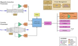
Figure 1 represents a system block diagram of a flow meter transmitter. Typical flow rate applications measure gases, vapors, and aggressive or viscous liquids in pipelines, as well as bulk solids on conveyor belts. The sensor electronics include a low-power microcontroller (MCU), high-precision data converters, input amplifiers, output drivers, isolation, connectivity options, and power management.
Two types of volumetric flow sensors, magnetic-inductive and Coriolis, are shown in Figure 1. Magnetic-inductive flow meters, commonly called magmeters, detect the flow rate of conductive media.1 The principle of operation is based on electromagnetic induction, whereby the conductive medium flowing through a pipe in a magnetic field generates a voltage proportional to the flow velocity or volumetric flow quantity. Meanwhile, Coriolis flow meters directly measure mass flow rate by determining the time difference or phase shift as a result of the twisting force caused by Coriolis acceleration.2
Note that the input, signal conditioning, and output subsystems in Figure 1 appear in other guises, as well. With a change of sensor transducer and suitable adjustments to the analog front-end (AFE) and MCU firmware, many other process variables can be measured. The sensor transmitter communicates data back to a centralized data aggregation point—for example, a programmable logic controller (PLC) host—via wired or wireless connectivity.
A commonly used wired-communication interface is the 4- to 20-mA current loop illustrated in Figure 2, the convenience being that power is also derived from this two-wire connection. Being able to program and communicate with sensor nodes remotely, and have them operate reliably for long periods of time on low power, are key considerations.
Supply Current Budget
While the MCU and data converters of a rudimentary sensor transmitter circuit are typically optimized for low operating current, the feature set and increased functionality of high-performance sensor applications lead to increased current demand. Such intelligent sensor systems may not be able to meet typical under-scale current thresholds or zero-scale level (4 mA) of the 4-20 mA current loop. NAMUR NE43, a widely adopted standard, interprets loop currents at and below 3.6 mA as a diagnostic failure information range.3
The result is that the total load current from the 4-20 mA loop is limited to 3.6 mA or lower and must be sufficient to power all functional blocks of the transmitter: sensor AFE excitation and interface, MCU for temperature non-linearity correction or other user-defined compensation algorithms, galvanic barrier jump to break ground loops, and DAC with 4-20 mA loop drive. Wireless connectivity options, such as Bluetooth Low Energy (BLE) or WirelessHART, provide calibration and remote diagnostic capability, but also contribute to increased current consumption.
To increase the available supply current for a loop-powered sensor transmitter, a DC-DC converter with high efficiency provides an inherent current multiplication feature not possible with a traditional linear regulator (LDO) solution. An increased current budget, above the nominal 3.6 mA, offers developers of smart sensor applications the flexibility to support advanced features.4
Loop-Powered Buck Converter
A synchronous buck converter can reliably power a transmitter circuit with higher current requirement, even at the minimum available input power condition when the transmitter is operating at its compliance voltage (that is, the lowest voltage between the LOOP+ and LOOP− terminals in Figure 2, typically 8V). Ultra-high efficiency within a 1 mA-to-20 mA output current range is imperative. To deal with supply rail transient voltages, a wide-VIN DC-DC solution in particular offers a larger voltage rating for additional operating margin.
For a synchronous buck converter with integrated MOSFETs that produces a tightly regulated output, even in volatile voltage environments, a 150-mA converter from TI offers high efficiency and ultra-low quiescent current, IQ.5 Operating from a 20:1 wide VIN range and capable of sustaining repetitive 65 V surges, the output voltage of the LM5165 is immune to large and noisy voltage swings at the input. Such transient immunity performance is critical in sensor applications where high reliability and extended product life cycle are essential.
Figure 3 shows the converter schematic with a switching frequency of approximately 350 kHz at nominal 24 V input. An input filter includes reverse polarity protection and surge protection. A 40-Ω sense resistor for the loop current is shown explicitly, but this is normally integrated into the loop driver.7 The power solution is easy to use, requiring no loop compensation components. The fixed output versions of 3.3 V and 5 V need only a filter inductor and two capacitors for operation, while an adjustable output version is configured with just two 0402 feedback resistors.
Implementation Specifics
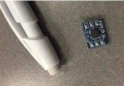
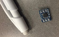
Solution footprint and height are critical in space-constrained sensor housings, meaning system designers must explore all avenues to conserve valuable printed circuit board (PCB) real estate. Figure 4 shows a converter implementation with small solution size using a standard four-layer FR-4 PCB. The package size and manufacturer’s recommended pad geometry of the essential converter circuit components are detailed in Table 1.
Various features integrated for reduced size and enhanced reliability include an internally-fixed or externally-adjustable output soft-start (SS), precision enable with customizable hysteresis for programmable line undervoltage lockout (UVLO), and an open-drain PGOOD indicator for sequencing and fault reporting. A cycle-by-cycle peak current limit threshold provides inherent fault protection from output overload and short circuits. Moreover, the peak current limit is adjustable such that smaller footprint inductor and capacitors function for high-density, low-current applications.
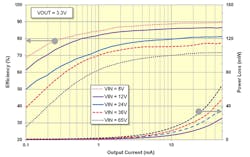
The plot of Figure 5 shows the converter efficiency with the output current plotted on a log scale from 100 µA to 50 mA. High efficiency is achieved at higher loads through optimized power MOSFETs switching, and continues at light loads by virtue of low IQ in both sleep and active operating modes combined with diode emulation and pulse-skipping to reduce switching activity and minimize switching power losses.
Tackling EMI and EMC
A key design requirement is to comply with electromagnetic compatibility (EMC) regulations.6 Table 2 lists the important EMC standards and suggested test levels for sensor applications. A resistor in series with the converter input, designated RIN1 in Figure 3, is typical for 4-20 mA current loop circuits. It provides damped electromagnetic interference (EMI) filtering and input ripple attenuation, as well as contributes to small-signal stability of the current loop. Additional high-frequency filtering is offered by ferrite beads designated LIN1 and LIN2 in Figure 3, each rated for an impedance of 600 Ω at 100 MHz.
The LM5165 uses an integrated active slew rate control of the switch-node (SW) voltage transition to reduce EMI filtering requirements. This improves both conducted and radiated EMI signatures.8-9 As shown in Figure 6, the current-source gate driver discharges the high-side MOSFET’s non-linear gate capacitance CGD so that the SW voltage overshoot and ringing are eliminated. Capacitance CGD increases as voltage VDS decreases, corresponding to SW voltage increasing, and the current-source gate-driver tunes the slew rate profile of the SW voltage as it swings from GND to VIN during the turn-on transition of MOSFET Q1.
The benefits of this switching scheme are increased reliability and robustness owing to lower voltage and current stress, increased margin for input voltage transients, reduced body diode reverse recovery charge from lower di/dt, more tolerance of non-optimized PCB layouts, and easier EMI filtering—particularly in the more challenging high-frequency band above 30 MHz.
References
1. Kalyanaraman, Deepa. “Industrial flow meters/flow transmitters,” Texas Instruments Analog Applications Journal (AAJ) 2Q 2012.
2. Mass flow meter, Wikipedia.
3. Hegarty, Timothy. “Powering smart sensor transmitter in industrial applications,” Texas Instruments Industrial Strength blog, May 2, 2016.
4. Hegarty, Timothy. “Low-IQ synchronous buck converter enables intelligent field sensor applications,” Texas Instruments AAJ 2Q 2016.
5. LM5165 3V-65V, 150 mA synchronous buck converter with ultra-low IQ, TI product folder, 2016.
6. Williams, Ian. “Electromagnetic compatibility testing explained,” TI Precision Hub blog, February 6, 2016.
7. DAC161S997 SPI 16-bit precision DAC for 4 to 20 mA loops, TI product folder, 2016.
8. K.W. Kam et al, “EMC guideline for synchronous buck converter design,” IEEE Int. Symposium on EMC, August 2009, pp. 47–52.
9. Bhargava et al. “DC/DC buck converter EMI reduction using PCB layout modification,” IEEE Trans. on EMC, August 2011, pp. 806–813.
About the Author
Timothy Hegarty
Systems Engineer in Non-Isolated Power Solutions
Voice Your Opinion!
To join the conversation, and become an exclusive member of Electronic Design, create an account today!

Leaders relevant to this article:


