eGaN® FET- Silicon Power Shoot-Out Volume 11: Optimizing FET On-Resistance
So far in this series, significant efforts have been made to show the performance improvements that can be achieved with eGaN® FETs over silicon MOSFETS in both hard and soft switching applications. In every case, eGaN FETs showed improvement over MOSFETs. In this volume of the eGaN FET-Silicon power shoot-out series, the die size optimization process is discussed and an example application is used to show specific results. ‘Optimum’ may mean different things to different people, so this process is aimed at maximizing switching device efficiency at a given load condition.
Device Losses Modeling
Initial shoot-out articles [1, 2] showed that eGaN FETs behave for the most part just like silicon devices and can be evaluated using similar performance metrics. Since these devices behave like silicon MOSFETs, they can also be optimized in a similar fashion; by balancing static and dynamic losses through adjusting die size. Static losses include loss components unaffected by changes in switching frequency, while dynamic losses are very much frequency dependent. An assumption is that all device parameters will scale with die size but that the device Figures of Merit (FOMs) will remain unchanged. Although applications may be varied, the different loss components are easily summarized [3, 4, 5]; only their relative sizes change with application and operating frequency. With eGaN FETs, the relative weights of the loss components will also differ from silicon MOSFETs and thus result in different ‘optimum’ die size values. To better understand this, lets first break down the total semiconductor losses within a power FET (PSEMI) as follows:
PSEMI = PCOND + PT-ON + PT-OFF + PDR + PQRR + PQOSS + PDIODE (1)
with the parameter descriptions given in Table 1.
Note that not all devices will have all these loss components, e.g. a synchronous buck converter would have practically no turn-on or turn-off losses in the synchronous rectifier. Furthermore, to optimize multiple devices in a converter, the losses stemming from the interaction between devices also need to be considered (e.g., the diode reverse recovery losses of one device may be dissipated in another FET. This occurs in circuits such as synchronous buck converters where synchronous FET related losses are dissipated in the control FET, but by optimizing the control FET only, this loss component will remain unchanged. Thus for optimization purposes, this issue is resolved by considering all the losses induced by a device to be relevant for its sizing, regardless of where the power is dissipated.
Die Size Optimization
By considering each of these device loss components in Equation (1) in turn, some conclusions can be drawn:
The conduction losses (item 1-parameter descriptions) are frequency independent
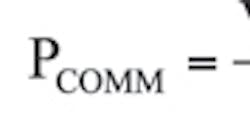
Commutation loss (items 2a and 2b-parameter descriptions) are both frequency and load current dependent and can be combined as follows as shown in Equation 2:
Where:
Loss components in items 3, 4 and 5 (parameter descriptions) are all frequency dependent, but current independent and can be combined. While QRR is current related, MOSFET vendors neglect to present their characteristics adequately over current, temperature and di/dt to accurately calculate these losses:
Diode losses, item 6 (parameter descriptions), are assumed die size independent (only a weak function of die size) and neglected for the optimization process.
If we now define two new variables DIEQ and DIEQRR as:
Then combining Equation (2) and Equation (3) and substituting Equations (4a) and (4b), the switching losses are shown in Equation 5:
Thus, the non-current dependent losses in Equation (3) can be modeled as an equivalent switching loss with an equivalent current DIEQRR for reverse recovery related losses, and DIEQ as the remaining charge related losses as defined in Equation (4). The QRR related losses term can be neglected for eGaN FETs where QRR is equal to zero, but is included for MOSFET compatibility. Thus from Equation (5) and item 1 from Equation (1), the total device losses for optimization purposes can be written as:
To find the optimum (minimum loss) point, we set the derivate to zero and calculate A:
If we normalize all charge values to 1 W RDS(ON), then the optimum device on-resistance is given by:
The normalized eGaN FET device specific parameters are given in Table 2 for a typical ‘hot’ operating temperature of 100 °C junction. Thus, with Equation (8) and the values from Table 2, the optimum required die resistance can be readily calculated for a given bus voltage.
This process may best be explained by example, but first the decision as what load conditions are to be used for optimization must be chosen. To explain this, consider the following sets of efficiency curves for the same application shown in Fig. 2.
- Full Load Optimization: will result in the best full load efficiency at the cost of reduced light load and peak efficiency.
- Medium Load Optimization: will result in the best medium load efficiency at the cost of full load efficiency. This is likely to result in the most ‘flat’ efficiency curve.
- Light Load Optimization: Best light load efficiency achieved at a significant cost of full load efficiency. May be useful where certain light load efficiency standards need to be met or minimum energy consumption standards need to be met.
Thus, the load current should be chosen based on where on the efficiency curve should peak (or as close as possible). This selection is complicated by the fact that the device losses are not the only current dependent circuit losses, i.e. bussing resistance and inductor DCR also increase quadratically with load current. Thus the die size optimization should be skewed towards higher dynamic losses to compensate, but with multiple devices each device can account for some arbitrary fraction of the total circuit resistance losses. If REQ is an equivalent circuit resistance to be compensated for, then the adjusted optimum on-resistance (ROPT-ADJ) is given by:
eGaN FET Optimization Example
Consider a high frequency buck converter with the following specifications [6]:
VIN = 45 V, VOUT = 22 V, fSW = 1 MHz, ILMAX = 30 A
For optimization, peak die or circuit efficiency is to be achieved at 15 A (50% load). From Table 2, we get DIEQ = 7.7 A, DIEQRR = 0 A, k = 1.44 /A and QSW,A = 28 pF / W (using the 48 V). Also needed are D = 22/45 = 0.49 and IL = 15 A.
For the adjusted optimum on-resistance, a total equivalent circuit resistance of 8 mW is estimated from [6]. Since the high-side control FET losses dominate total device losses, let’s arbitrarily choose 7 mW of this be compensated for in the high-side. Since equivalent resistance losses are compensated by increasing switching losses, it makes sense to compensate most (if not all) of these losses in the device with higher switching loss.
Control FET Optimization
For the control FET, the on-state duty cycle is ‘D’, there are no QRR losses, but there are QOSS and hard switching losses. From Equation (8) we get the values for ROPT, as shown in Equation 10:
where ROPT(25 °C) = ~9.7 mW typical
Considering the equivalent circuit resistance, the adjusted optimum on-resistance is from Equation 11:
where ROPT-ADJ(25 °C) = ~5.7 mW typical
Synchronous FET Optimization
For the synchronous FET, the load current IL at switching is taken as zero, while there are no turn-on or turn-off commutation losses in the synchronous FET, QOSS induced losses and QRR losses are present (zero for eGaN FET). Also the on-state duty cycle is ‘1-D’. Thus from Equation (8) we get Equation (12) below:
where ROPT(25 °C) = ~5.2 mW typical
Considering the equivalent circuit resistance, the adjusted optimum on-resistance is shown in Equation (13) in the left-hand box, for the remaining 1 mW:
where ROPT-ADJ(25 °C) = ~4.3 mW typical
As can be seen from this example, the optimum on-resistance changes significantly for any large (same range as the device on-resistances) additional circuit resistance being compensated for. Obviously, these additional circuit losses could be minimized prior to compensation and any such additional optimization adjustment would be minor. To see the impact of adjusting for some of the equivalent circuit resistance, the control FET and synchronous FET optimum resistance are plotted versus load current for this same example in Fig. 3 and Fig. 4, respectively.
Experimental Results
To evaluate the validity of this optimization approach, some experimental efficiency curves were taken for the same buck converter used in the example above [6]. The same circuit was built and only the EPC devices were changed, as outlined in Table 3, using various combinations of the EPC2001 [7] and EPC2016 [8] eGaN FETs. The efficiency and power loss curves as function of load current for these three cases are plotted and shown in Fig. 5. Their estimated optimized points are color coded and added as dots to Fig. 3 and Fig. 4. Table 3 shows good correlation between the adjusted on-resistance and actual current levels at peak efficiency.
Optimization Comparison with MOSFETs
To see how this optimization process compares when using MOSFETs, it is necessary to find representative high performance MOSFETs and normalize them in a similar manner. The resultant values are given in the appendix, Table 5 for reference. Using the same design example as before, the resultant optimum on-resistance values for the control and sync FETs are plotted versus load current in Fig. 6 and Fig. 7, respectively. The reverse recovery losses (QRR) for these MOSFETs taken from the datasheets are rather large and could be mitigated by the addition of a freewheeling Schottky diode. Therefore, the resultant MOSFET on-resistance, neglecting QRR losses, is also shown in Fig. 7. This graph clearly shows the similarity between eGaN FETs and MOSFETs and shows that an optimal eGaN FET would have a lower resistance than a similarly optimized MOSFET device. This results from the reduced dynamic losses offered by the eGaN FET due to its lower FOM [1].
Effect of Package and Layout on Optimization
It has been shown [9, 10, 11] that common source inductance (CSI) will significantly increase switching loss for hard switching devices. Equations for the estimation of this increase are complex and somewhat varied. This loss increase, although significant has also been shown die size independent for a given device technology [12] and therefore has little impact on die size optimization process. For eGaN FETs in practice, however, the CSI would be a weak function of die size as all the wafer level chip-scale package (WLCSP) inductances will scale with die size, but this complexity is beyond the scope of this paper. Such an inverse relationship between CSI and die size means that some small portion of switching losses actually decreases with increasing die size, even though this may seems counter intuitive.
Using the simple optimization method presented here is a quick way to find the optimum eGaN FET on-resistance value. As with many simple solutions, the accuracy is limited and the actual optimum resistance may deviate. Furthermore, the optimum combination of die size and on-resistance is also a function of the non-device related equivalent circuit conduction resistance.
Since eGaN FETs will always optimize to a lower on-resistance than MOSFETs, the overall peak efficiency will therefore be higher than MOSFETs. If the same on-resistance is used, the eGaN FET efficiency will peak at a lower current.
References:
- J. Strydom, “eGaN® FET-Silicon Power Shoot-Out Part 1: Comparing Figure of Merit (FOM)”, Power Electronics Technology, Sept. 2010.
- J. Strydom, “The eGaN FET-Silicon Power Shoot-Out: 2: Drivers, Layout”, Power Electronics Technology, Jan. 2011.
- Jon, Klein, “Synchronous buck MOSFET loss calculations with Excel model”, Fairchild Semiconductor, App. note AN-6005.
- Jon Gladish, “MOSFET Selection to Minimize Losses in Low-Output-Voltage DC-DC Converters”, Fairchild Semiconductor Power Seminar 2008 – 2009.
- “Properly Sizing MOSFETs for PWM Controllers”, Sipex App. note ANP-20.
- J. Strydom, “eGaN® FET- Silicon Power Shoot-Out Volume 8: Envelope Tracking”, Power Electronics Technology, Apr. 2012.
- EPC2001 datasheet, EPC Corporation.
- eGaN FETs Product Selector, EPC Corporation.
- D. Jauregui, B. Wang, R. Chen, “Power Loss Calculation with Common Source Inductance Consideration for Synchronous Buck Converters”, Texas Instruments, SLPA009A, June 2011.
- W. Eberle, Z. Zhang, et. al, “A Practical Switching Loss Model for Buck Voltage Regulators”, IEEE Transactions on Power Electronics, Vol. 24, No. 3, March 2009.
- T. Hashimoto, M. Shiraishi, et. al, “System in Package (SiP) With Reduced Parasitic Inductance for Future Voltage Regulator”, IEEE Transactions on Power Electronics, Vol. 24, No. 6, June 2009.
- Y. Ying, “Device Selection Criteria - Based on Loss Modeling and Figure of Merit”, M.Sc. Thesis, Virginia Tech.
Related Articles:
Enhancement Mode GaN MOSFET Delivers Impressive Performance
600 V GaN on Si-Based Power Use GaNpowIR®
About the Author
Comment About the Article
To join the conversation, and become an exclusive member of Electronic Design, create an account today!

Leaders relevant to this article: