eGaN® FET- Silicon Power Shoot-Out: Small Signal RF Performance
Unlike power switching FETs, RF FETs are designed to work best in the linear region of operation to maximize power gain and minimize distortion, whereas power switching devices are optimized for lowest RDS(ON) and gate charge[1,2,3,17,18,19,20]. Another significant difference between power switching and RF FETs is the power dissipation capability of RF devices is significantly higher than that of power switching devices for equivalent terminal characteristics to accommodate the higher power losses in the linear region.
We will focus on RF characterization in the frequency range from 200 MHz through 2.5 GHz, the results of which can be used to design a pulsed power RF amplifer.
RF Characterization
Prior to being able to compare various RF FETs with each other they need to be properly characterized, which can accomplished by measuring the S-parameters of the FET while regarding it as a 2-port network under controlled bias conditions.
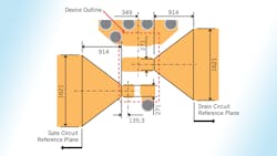
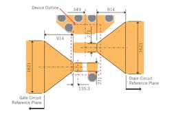
A test fixture was designed for the EPC2012 to connect the RF signals to the FET and to provide the necessary S-parameter measurement reference planes from which the dataset would be valid. The test fixture design used a 30 mil thick Rogers 4350 substrate [21], chosen for its low losses at higher frequencies. This allowed the design to be suitable for frequencies as high as 12 GHz. Fig. 1 shows the reference plane design and highlights the outline of the EPC2012 device. The transmission lines to the device Gate and Drain were designed as microstrip transmission lines with 50 Ω characteristic impedance.
Related Articles
- GaN Transistors: Thermal Management, Drive Control and Isolation
- Characterizing High Power Semiconductors Requires New Technologies
- Quality, Robustness and Reliability of 600 V GaN-on-Si Power Devices
- Cascode Configured GaN Switch Enables Faster Switching Frequencies And Lower Losses
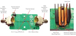
The test fixture was also equipped with a negative temperature co-efficient thermistor (NTC) placed in close proximity to the source pad of the eGaN FET to provide an indication of the temperature of the copper in that area without affecting the RF performance. The EPC9903 test fixture in Fig. 2 shows the right side image showing the top mounted heat-sink. The EPC FET has a lower thermal resistance [3] from junction to the top side of the device, compared to the bottom side (soldered), and hence mounting the heat-sink to the back side of the device has a high impact on the power dissipation capability of the device.
Due to thermal limitations of the test fixture and the EPC2012 device, testing of the eGaN FET was pulsed with a low duty cycle with the average power dissipation kept below 0.7 W without the heat-sink, and 5 W with the heat-sink and forced air cooling. The heat-sink used was 15 mm x 15 mm x 14.5 mm high, supplied by Advanced Thermal Solutions [14] with thermal interface material from Wakefield [7].
RF Measurement
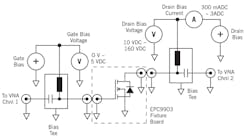
The basic setup using the EPC9903 test fixture is shown in Fig. 3. Both the bias and RF signal are provided to the board using SMA connectors. A bias Tee [4] was used for the separate connection of gate/ drain bias and the RF signal.
Prior to using the test fixture (EPC9903) for the S-parameter measurement of the EPC2012 device, it was calibrated using the Thru-Reflect-Line (TRL) method [10]. The process followed is well documented and similar to that described in [11].
With the small signal S-parameter setup complete, the next step was to measure the EPC2012 device at various bias conditions to determine the highest maximum gain bias point. This will then be used to design a class A power amplifier to evaluate the RF power performance of the EPC2012.
Initial testing to determine the useful gain frequency range of the device swept the frequency from 30 MHz through 12 GHz under continuous wave (CW) conditions at a low drain bias voltage of 10 V and 300 mA. Subsequent testing was limited to the 200 MHz through 2.5 GHz frequency range. Initial testing also investigated the influence of the heat-sink on the RF performance of the test fixture and the device. It was found that the impact of the heat-sink only became detectable at frequencies above 2.5 GHz and caused a resonance around 6.5 GHz which is well above the working frequency of the device.
Various drain bias conditions were then applied to the FET terminals from 10 V through 70 V, and from 10’s of mA though 6 A as small signal S-Parameter measurements were taken. Under these conditions the bias power dissipation in the FET became significant and therefore the device was pulsed for short durations while measurements were taken. The pulse width was set to approximately 20 µs with a repetition frequency of 50 Hz.
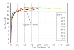
For this discussion, the gate-source circuit will be designated as port-1 and the drain-source circuit as port-2. Maximum gain at 500 MHz is shown in the graph (Fig. 4) as a function of drain bias power. The graph clearly shows that once the drain bias power exceeds 20 W there is very little increase in maximum gain with further increase in drain bias power. It also shows a nearly constant gain with drain voltage beyond 15 V bias. The graph shows the useful drain bias power range for a class A amplifier highlighted by the region of interest and will be the design point for such an amplifier. It is important to note that, for an amplifier design the drain bias must have sufficient voltage to allow the drain to swing with maximum amplitude. Too high of a voltage will lead to unnecessary drain bias power, and too low of a voltage will reduce the 1 dB compression point and induce clipping.
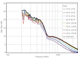
Fig. 5 shows a graph of maximum gain as a function of frequency for various drain bias power conditions ranging from 10 W through 179 W. It should be noted that low drain bias power reduces the gain more above 600 MHz and, at very high drain bias power, gain reduces below 400 MHz.
Three optimal drain bias points have been identified from the data that will be used to evaluate the performance of the EPC2012 device as a class A amplifier operating at 500 MHz. The drain voltage is around 65 V with drain power of 20 W, 40 W and 80 W. The 500 MHz point was chosen as it yielded the highest gain frequency product for various devices tested. The various drain bias power points will be used to determine the impact on the 1 dB compression point and drain efficiency.
RF Power Amplifier Design
Suitable drain bias points and frequency have been selected for the EPC2012 device based on maximum gain and frequency. The S-parameters at these bias points and frequency that can be used in the design of an RF Power amplifier will be analyzed next.
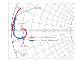
Fig. 6 shows the Smith Chart plot for the gate (S11) and drain (S22) reflection coefficients from 200 MHz through 2.5 GHz with a drain bias of 64 V and 1.275 A. A change in drain current has negligible impact on the input and output impedances. However, a reduction in drain voltage to below 15 V will have a significant impact on the input and output impedance as the COSS of the eGaN FET increases dramatically. This will also reduce the available gain as more output current is shunted internally in the device reducing the output voltage swing. This leads to non-linear behavior and must be accounted for in an amplifier design.
The Smith chart plot shows that the EPC2012 device has low impedance for both the gate and drain circuits in the frequency region from 200 MHz through 2.5 GHz, and of particular interest at 500 MHz where both are capacitive.
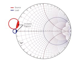
Based on measurement data, at a frequency of 500 MHz the gate-source impedance is 5.44 – j3.69 Ω and the drain-source impedance is 3.13 – j3.08 Ω and can be used to determine matching networks for the device. The impact of bias networks, and whether an amplifier must be unconditionally stable, must also be considered prior to matching network design.
Since the real part of both the gate-source and drain-source impedances are smaller than the characteristic impedance of the transmission lines (50 Ω) used to connect the RF signal to the eGaN FET, the impedance matching network will take the form shown in Fig. 8.
The basic matching network shown in Fig. 8 has the following solutions [1]:
Where:
Zo = Characteristic impedance of the transmission line used to connect the RF signal to the eGaN FET.
ZL = Gate-source or drain-source impedance
RL = Resistance part of ZL
XL = Reactance part of ZL
B = Matching shunt reactance
X = Matching series reactance
A trombone section of the input microstrip transmission line can be used to tune the impedance matching network to the device at a specific frequency whereby a shunt matching component may be installed anywhere along its length. Using the calculated value for B (Fig. 8),which in this case will be a capacitor, and moving it away from the FET on the 50 Ω transmission line, rotates the impedance clockwise on the Smith Chart with the result of shifting the impedance and altering the frequency response of the matching network. This is useful when designing an amplifier suitable for a wide operating frequency range.
Applications
S-Parameter analysis of the EPC2012 eGaN FET has demonstrated that at up to 635 MHz, the device exhibits a good gain (>10 dB). This makes it useful for several applications, and in particular pulsed applications. These applications include Magnetic Resonance Imaging (MRI) Low power transmit systems and cyclotron drivers.
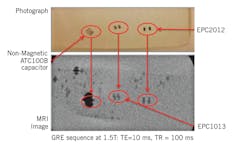
MRI systems operate in the frequency range from 42 MHz (1T systems) through 300 MHz (7T systems). During imaging, an RF pulse is transmitted into the subject. The EPC2012 has several electrical characteristics that make it suitable for use in MRI transmit systems. A magnetic susceptibility test was conducted by Case Western University to further determine if the EPC2012 was also suitable for use inside the MRI magnet. Any component inside the magnet must have an absolute volumetric magnetic susceptibility value of less than 24·10-6. Fig. 9 shows an MRI and photograph images from the magnetic susceptibility test and clearly shows that the EPC device has no impact on the image quality and is clearly distinguishable in the MRI image. A device which exceeds the magnetic susceptibility limits will distort the image and will clearly show up as either a large black spot or produce ripples on an image similar to a stone thrown in water.
Cyclotron Driver
Another application that is suitable for the EPC2012 device is a cyclotron driver. Such systems operate over a wide range of frequencies and are typically application specific. Cyclotrons are also pulsed and, due to the EPC2012’s small size and high voltage rating, are ideally suited for these types of applications [2]. Future work may also explore applications such as WiFi, Bluetooth, Zigbee and M2M power amplifiers which all operate in pulse mode.
For continuous wave (CW) applications, the EPC2012 device would need to be in an appropriate RF package that is capable of dissipating large amounts of heat flux. Another option for the efficient removal of heat from the RF package is eutectic die attach of the eGaN FET back side silicon directly to the circuit board substrate.
Acknowledgements
EPC hereby acknowledges the following for their support during this project:
• Modelithics Inc. for their support in the design of the test fixtures and measuring the small signal S-Parameters.
• Michael Twieg and Mark Griswold, Case Western Reserve University - Case Center for Imaging Research, for their assistance with the magnetic susceptibility testing of the EPC2012 eGaN FETs
• The blank Smith chart courtesy of www.RFcafe.com.
• M. Meiller, Peakgainwireless, for help with s-parameter analysis that lead to the matching network design
References
[1] D. M. Pozar, “Microwave Engineering”, Third Edition 2005, J. Wiley ISBN 0-471-44878-8
[2] http://en.wikipedia.org/wiki/Cyclotron
[3] EPC2012 datasheet, www.epc-co.com
[4] Bias Tee 8860SFM2-12, www.aeroflex.com
[5] S. J. Orfanidis, “Electromagnetic Waves and Antennas”, Chapter 13, http://www.ece.rutgers.edu/~orfanidi/ewa/
[6] www.rfcafe.com
[7] Wakefield Engineering thermal interface material P/N 173-7-1212A, http://www.wakefield.com
[8] http://en.wikipedia.org/wiki/Electronic_amplifier
[9] R. C. Hejhall, “RF Small Signal Design Using Two-Port Parameters”, Motorola application note AN215A, 1993.
[10] Engen, G.F., Hoer C.A.,“Thru-Reflect-Line: An Improved Technique for Calibrating the Dual Six-Port Automatic Network Analyzer,” IEEE Trans. Microwave Theory and Techniques, December 1979.
[11] Agilent Network Analysis Applying the 8510 TRL Calibration for Non-Coaxial Measurements Product Note 8510-8A
[12] www.microwaves101.com
[13] http://en.wikipedia.org/wiki/Magnetic_susceptibility
[14] ATS-54150K-C2-R0 datasheet, Advanced Thermal Solutions, www.qats.com
[15] Ken Payne, “Practical RF Amplifier Design Using the Available Gain Procedure and the Advanced Design System EM/Circuit Co-Simulation Capability”, Agilent Technologies White Paper, 2008, www.agilent.com
[16] G. Gonzales, “Microwave Transistor Amplifiers”, Second Edition 1997, Prentice Hall ISBN 0-13-254335-4
[17] A. Lidow, J. Strydom, M. de Rooij, Y. Ma, “GaN Transistors for Efficient Power Conversion”, First Edition, ISBN 978-0-615-56925-3
[18] J. Strydom, “eGaN® FET- Silicon Power Shoot-Out Volume 8: Envelope Tracking”, Power Electronics Technology, May 2012, http://powerelectronics.com/power_semiconductors/gan_transistors/egan-fet-silicon-power-shoot-out-volume-8-0430/
[19] J. Strydom, “eGaN® FET- Silicon Power Shoot-Out Volume 11: Optimizing FET On-Resistance”, Power Electronics Technology, Oct. 2012, http://powerelectronics.com/discrete-semis/gan_transistors/egan-fet-silicon-power-shoot-out-volume-11-optimizing-fet-on-resistance-1001/
[20] M. de Rooij, J. Strydom, “eGaN® FET- Silicon Power Shoot-Out Volume 9: Low Power Wireless Energy Converters”, Power Electronics Technology, June. 2012, http://powerelectronics.com/discrete-power-semis/egan-fet-silicon-shoot-out-vol-9-wireless-power-converters
[21] Rogers 4350 material specifications, www.rogerscorp.com
[22] J. M. Rollett, “Stability and Power-Gain Invariants of Linear Twoports”, IRE Transactions on Circuit Theory, Vol. 9, Issue 1, March 1962, pp 29 – 32
Voice Your Opinion!
To join the conversation, and become an exclusive member of Electronic Design, create an account today!

Leaders relevant to this article:
