Four-Pin TO Type MOSFET Package Lowers Switching Losses
For many recent generation power semiconductors, package innovation makes a significant contribution to key performance parameters. In the case of HV MOSFETs, high-speed hard-switching transitions are limited by the package source-inductance because the MOSFET drain current and gate current share a common path. Eliminating the influence of this source inductance by moving from a three-pin package to four-pin resulted in a power savings of 8 W in a demonstration design.
Related Articles
- P-Channel MOSFETs Come In PowerPAK® Packages
- High-Efficiency Power Family Uses New Energy-Saving Package
- MOSFET Packages Offer Cooler Operation
- Low-Side MOSFET Driver in Ultra-Small Four-Pin Package
In the latest generation of high voltage Super Junction (SJ) MOSFETs, the historic silicon transition time value (di/dt) is no longer a performance limiter. Instead, parasitic source inductance of the chip package limits transition time, because in the typical three-pin package the drain current and gate current share a common path. A novel approach to dealing with this performance limiter is to add a fourth pin to the commonly used package types. Based on both simulation and measured results on a test board, this method of eliminating switching loss incurred by source inductance is seen to improve efficiency and lower die temperature.
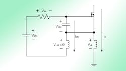
A simple example characterizes the impact of parasitic source inductance on switching loss. This example assumes an intrinsic parasitic source inductance of 2nH. (NOTE: The figure for a standard TO-247 three-pin is ~8 nH and a typical HV leadless SMD package such as ThinPAK8x8 has an inductance of 1.5 nH). Driving the gate with a standard VDRV = 12 V and assuming a Vplateau in the range of ~5 V during current commutation (fairly typical value), we arrive at:
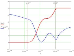
A simulation based on these conditions at a ~5 Ω total gate resistance (3.4 WRg,ext + 0.5 Wdriver output impedance + 0.82 WRg,int), produces the Id waveform illustrated in Fig 1.
The underlying fundamental di/dt limit is around 25 A/9 ns or ~2.8 A/ns – and the gate current goes to 0 at max VLS. Turn-on energy of ~71 mJ is observed (from simulation).
A Separate Path
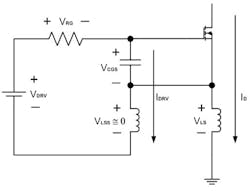
In an approach we named Source-Sense a TO-247 packaged HV MOSFET was implemented with a fourth pin, which creates separate paths for the gate current and drain source current. With separation of the current paths, as seen in Fig. 2, di/dt only causes a voltage drop across the “Power Source” package inductance; VLS. Since VDRV and VCGS are both close to constant, VRG will also be close to constant, and the current through the loop will therefore also be close to constant (di/dt ~ 0); causing VLSS to be approximately 0 volts.
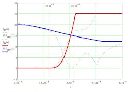
With the effect of package parasitic source inductance completely averted, the simulation reviewed earlier was repeated, with the results seen in Fig. 3.
The di/dt achieved in this case is steeper than ‘allowed’ by source inductance. The gate current in the 4-pin case only reduces as VGS rises (as would be expected) with no feedback contribution from LS.
The resulting di/dt of roughly 25 A/5 ns corresponds to 5 A/ns, which is almost double that of the alternative three-pin configuration.
Turn-on energy of ~18 microJoule is observed, which equates to a net energy savings of 53 mJ compared to the three-pin scenario. Assuming ~40% operation near 25 A peak for a sinusoidal wave-shape and a switching frequency of 100 kHz, this power savings equates to ~2.6 W in a typical 2.5 kW PFC application. Not only would the demands on the thermal management system become more relaxed, but a net efficiency increase on the order of 0.2% at low line (~1150 W POUT) is a welcomed benefit onto itself.
Physical Measurements
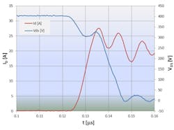
Based on the positive results in simulation, a test board was constructed in a way that a typical three-pin package could be directly compared with the Source-Sense approach, with no changes made other than the added pin. ID as well as VDS was documented in both cases for direct A/B comparison. The first measurements were made with a CoolMOS C7 SJ MOSFET in a TO-247 3-pin package (Fig. 4).
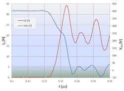
In changing to a 4-pin source-sense package implementation, we expect to see a direct efficiency improvement with higher di/dt and monotonically decreasing VDS. (Fig. 5).
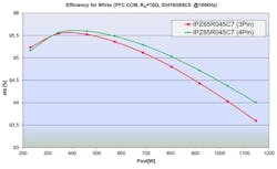
In comparing Fig. 4 and Fig. 5, a monotonically decreasing VDS is observed as well as higher di/dt with a much shorter total transition time. The resulting effect on efficiency is a function of current magnitude (di/dt limiting for three-pin devices is worse at higher current magnitudes), and we should therefore expect less difference at light loads and a much bigger efficiency gain at full load. To confirm this, efficiency of the two devices at different load levels was measured, as seen in Fig. 5.
We can see that faster switching transients translate to a tangible efficiency gain even at 50 percent load and at full load of 1150 W output this increases to a 0.4 percent improvement; equal to a power dissipation difference in the switching MOSFET of ~5.2 W. In addition to lower overall losses, this reduction can have a tangible impact on heat sink requirements in a design.
The observed differences between test board measurements and simulation are expected for several reasons. First, the TO-247 device was partially inserted onto the board, which means effective source inductance likely somewhat higher than the assumed 2 nH. The use of different RG can also be expected to have an impact, as can the difference between an ideal gate driver in case of the simulation and an existing physical one.
Design Impact
Implementation of four-pin HV MOSFET package does entail consideration of several other elements of system design. For example, a differentially driven VGS means that the driver-side can no longer be ground referenced to the same common (GND) potential as the load and BUS capacitor. This is similar to the needs in a high-side MOSFET of a half- or full-bridge configuration. Known strategies to address the Common Mode voltage spike incurred on the entire driver loop may also be applied. Both considerations are addressed in some detail in an Infineon Application Note [AN 2013-05, V1.0 May 2013].
Another way to address this voltage spike is to use a package with lower intrinsic source-inductance such as is offered in the ThinPAK 8 x 8 leadless SMD package that also employs the source-sense concept. Voltage drops during MOSFET turn-off that are controlled to some extent by the feedback mechanism of the combined current branch in the three-pin implementation may cause undue voltage stress to the MOSFET or diode. A leadless SMD package is useful to manage this challenge also.
Today, the classic TO-247 package can accommodate a physically larger chip than a leadless SMD, so designs meeting the most rigorous thermal performance or lowest possible RDS(on) will remain within that package class. Moving forward, more advanced package concepts will likely combine excellent thermal capabilities – possibly double-sided cooling for added engineering freedom – with large die size accommodations and the Source-Sense concept in a leadless SMD package that achieves a low total series inductance between drain and source for better total commutation loop inductance optimization.
About the Author
Voice Your Opinion!
To join the conversation, and become an exclusive member of Electronic Design, create an account today!

Leaders relevant to this article:
