Gate Drive Optocouplers Drive SiC Power Semiconductors
Silicon Carbide (SiC) power semiconductors are rapidly emerging in the commercial market. These devices offer several benefits over conventional Silicon-based power semiconductors. SiC MOSFETs can improve overall system efficiency by more than 10%, and the higher switching capability can reduce the overall system size and cost.
Related Articles
- Silicon Carbide (SiC) Power Module Family Expands
- Silicon Carbide Diodes Promise Benefits for Solar Microinverters
- High-Frequency Power Module is First to Use All Silicon Carbide
- Low-Loss Silicon Carbide (SiC) Power Devices
- 50 Amp Silicon Carbide Power Devices
- Silicon Carbide Schottky Diodes Push the Performance Envelope
Avago Technologies gate drive optocouplers are used extensively to drive Silicon-based semiconductors like IGBT and Power MOSFETs. Optocouplers are used to provide reinforced galvanic insulation between the control circuits from the high voltages and the power semiconductors. The ability to reject high common mode noise (CMR) will prevent erroneous driving of the power semiconductors during high frequency switching. We will discuss how the next generation of gate drive optocouplers can be used to protect and drive SiC MOSFETs.
Silicon Carbide is a wide bandgap (3.2 eV) compound. Wide-bandgap SiC, besides being able to operate at high voltage, frequency and temperature, exhibits on-resistance and gate charge by an order of magnitude lower than silicon material. In an evaluation conducted by CREE to compare the second generation 1200 V/20 A SiC MOSFET with a silicon high speed 1200 V/40 A H3 IGBT using a 10 KW hard-switching interleaved boost dc-to-dc converter, the results showed that even with five times the switching frequency, the SiC solution was able to achieve a maximum efficiency of 99.3% at 100 KHz, reducing losses by 18% from the best efficiency of the IGBT solution at 20 KHz.
CREE’s recent release of the C2M family of MOSFETs give engineers a wide range of competitively priced 1200 V and 1700 V SiC MOSFETs for a wide range of applications. Cree has been able to bring the MOSFET’s cost down significantly, while providing improved switching performance and lower Rds (on). Increasing the switching frequency can significantly reduce the size of the inductor. The lower conduction and switching losses allow engineers to reduce the size of the heat sink, or potentially remove fans and move to passive cooling solutions. Although a SiC semiconductor costs more than Si, the overall system BOM costs can be lower than Si technology by 20%.
SiC MOSFET Market and Adoption
SiC technology is now widely recognized as a reliable alternative to silicon. More than 30 companies worldwide have established SiC technology manufacturing capability with related commercial and promotional activities. Many power module and power inverter manufacturers have included SiC in their roadmaps for future products.
Solar inverter manufacturers and Server power supplies are the earliest adopters of SiC semiconductors as efficiency is critical in their technological ranking. In 2013, Europe’s top solar inverter makers, REFU, SMA and Delta announced a new model with SiC inside. Photon magazine evaluated SMA SiC inverters and efficiency increased from 98% to 99%, while the inverters’ physical weight was reduced by 30% as compared to equivalent IGBT inverter. The ramp-up of SiC semiconductor production will increase adoption in applications like motor drives, railway traction industrial uninterruptible power supplies, and hybrid vehicles.
Avago Technologies’ gate drive optocouplers have been used extensively to drive Silicon-based semiconductors like IGBTs. The company has been working closely with SiC market leader CREE Inc, to determine suitable gate drive optocouplers to fit SiC MOSFET operations. We have evaluated gate drive optocouplers ACPL-W346 and ACPL-339J with CREE C2M SiC MOSFET using an 8 A SEPIC dc-to-dc C cconverter at 100 kHz. The gate driving capability of these optocouplers met CREE’s efficiency requirement of 98% as indicated in Fig 1.

To match the low switching loss of CREE’s SiC MOSFET, the gate driver must be able to deliver high output current and voltage with fast slew rate to overcome the gate capacitance of the SiC MOSFET. The scope capture in Fig. 2 shows ACPL-W346 with a 20 V, fast rise and fall times signal profile at the gate of the SiC MOSFET which is necessary to switch the SiC MOSFET efficiently.

The ACPL-W346 (Fig. 3) is a basic gate driver optocoupler used to isolate and drive the SiC MOSFET operating at high DC bus voltage. It has a rail-to-rail output with 2.5 A maximum output current.
The ACPL-W346’s unique feature is its high speed -- currently the industry’s fastest in its class. The device’s maximum propagation delay is 120 ns and typical rise and fall times are around10 ns.
The ACPL-W346’s very high CMR, common mode rejection of 50 kV/µs is required to isolate high transient noise during the high frequency operation from causing erroneous outputs. When coupled with a bipolar current buffer stage, the device provides fast switching high voltage and high driving current to turn-on and off the SiC MOSFET efficiently and reliably. Compared to the older reference designs that employed a dedicated MOSFET driver with proprietary circuitry, the ACPL-W346 and the generic off-the-shelf bipolar current buffer offer a less expensive, easy to implement gate drive solution.
Driving and Protecting SiC MOSFETs
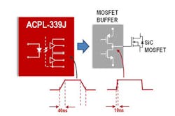
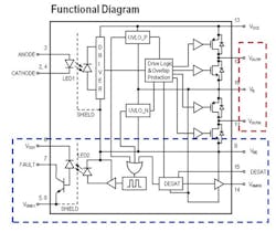
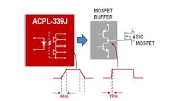
The ACPL-339J is a “smart” gate drive optocoupler that can isolate, drive and protect SiC MOSFET in a single chip solution. In the functional diagram Fig. 4, the integrated SiC MOSFET short circuit detection and faults feedback features are highlighted in blue. It has the industry’s first dual-output gate drive optocoupler uniquely designed to support the MOSFET buffer in the area highlighted in red. The device has a minimum output peak current of 1 A optimized for driving both high-side and low-side MOSFET buffer stage. It features an internal active timing control circuitry preventing cross conduction and minimizing switching losses in the MOSFET buffer stage.
The main reason for using MOSFET buffers, which comprise PMOS and NMOS transistors, is because they are voltage-controlled devices. The MOSFET’s output is able to switch very fast once its input threshold voltage (typically 1 V) is crossed. This way, the MOSFET buffer’s level switching speed is independent of the previous gate drive optocoupler stage’s level switching speed as shown in Fig. 5.
The scope capture in Fig. 6 shows ACPL-339J with bi-directional, fast rise and fall times signal profile at the gate of the SiC MOSFET, which is necessary to switch the SiC MOSFET efficiently.

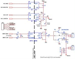
To execute the short circuit protection, the drain-source voltage of the SiC MOSFET is monitored by ACPL-339J (Fig. 7) during normal operation. When a short circuit occurs, high current flows through the SiC MOSFET and causes the drain-source voltage to increase rapidly. Once it crosses the ACPL-339J’s threshold of 8V, a short circuit fault is registered and soft shutdown is triggered. The ACPL-339J’s VGMOS pin will switch on an external transistor to slowly discharge the gate of the SiC MOSFET to achieve the soft shutdown effect. The entire short circuit protection is completed by reporting the FAULT through the insolated feedback path to the controller.
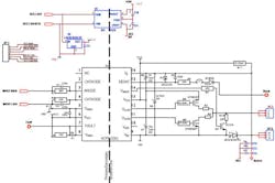
During a short circuit, high overload current together with any parasitic induced current can result in high overshoot voltage if the SiC MOSFET is shutdown abruptly, which could be exceeding the SiC MOSFET breakdown voltage. To minimize such damaging overshoot voltage, ACPL-339J does a soft shutdown when short circuit is detected. SiC MOSFET gate voltage is slowly reduced to low level off-state. The rate of soft shutdown can be adjusted through external MOSFET and resistance (Q3 and R10 in Fig. 7) to reduce the overshoot voltage level.

Fig. 8 shows the SiC MOSFET ‘s high overshoot and ringing across the drain-source of when doing a hard (or abrupt) shutdown during short circuit. (A low BUS voltage is used to prevent excessive damage to the SiC MOSFET during the experiment.) Fig. 9 shows how the high overshoot can be suppressed when the short circuit detection is triggered and gate is shutdown “softly.”

References
1. Dr Scott Allen,“Silicon Carbide MOSFETs for High Powered Modules,” CREE Inc., March 19, 2013.
2. Jimmy Liu, Kin Lap Wong, Scott Allen, John Mookken, “Performance Evaluations of Hard-Switching Interleaved DC/DC Boost Converter with New Generation Silicon Carbide MOSFETs,” CREE Inc.
3. “SiC Market 2013,” I-Micronews, May 25 2013.
4. Alexandre AVRON, “Overview of Wide Band Gap semiconductors in power electronics,” YOLE Développement, April 17, 2013.
5. “ACPL-P346 and ACPL-W346 2.5 Amp Output Current Power & SiC MOSFET Gate Drive Optocoupler with Rail-to-Rail Output Voltage in Stretched SO6 Package, ” Avago Technologies, AV02-4078EN.
6. “ACPL-339J Dual-Output Gate Drive Optocoupler Interface with Integrated DESAT Detection, FAULT and UVLO Status Feedback,” Avago Technologies, AV02-3784EN.
Comment About the Article
To join the conversation, and become an exclusive member of Electronic Design, create an account today!

Leaders relevant to this article: