IGBT Gate Drive Optocoupler Maximizes Design Flexibility

The ACPL-339J is more than just an optocoupler, it also includes short circuit protection, under voltage lockout (UVLO), “soft” IGBT turn-off, and isolated fault feedback to provide maximum design flexibility and circuit protection. It is an intelligent IGBT gate driver that constantly monitors its output power supply. If the output power supply is lower than its UVLO threshold, gate driver output will shut off to protect IGBT from low voltage bias. It has two UVLO logic blocks, UVLO_P and UVLO_N to control the VOUTP and VOUTN respectively. The UVLO control logic takes precedence over input IF and DESAT. In other words, IF and DESAT are ignored when VCC2 and VEE supplies are not sufficient causing UVLO clamp to be active. Both VUVLOP+ and VUVLON+ will need to be crossed before the clamps can be released. Thereafter, VOUTP and VOUTN will respond to IF and DESAT accordingly. Fig. 1 illustrates the SPICE simulation plots for the ACPL-339J.

Related Articles
- Liquid Metal Battery Stores Power After Sun Or Wind Retreat
- Organic Mega Flow Battery Promises Breakthrough For Renewable Energy
- University Researchers Pursue Better, Safer Li-Ion Batteries
- Inverter/Charger Supports Grid-Interactive and Off-Grid Applications
- North Carolina State Improves Lithium-Ion Batteries and Stacked Solar Cells
- Carbon Nanotubes: Flexible Battery, Computer, What Next?
Shown in Fig. 1, the Axion battery is a multi-celled asymmetrically supercapacitive lead-acid-carbon hybrid battery. Like the conventional lead-acid battery, the Axion battery consists of a series of cells. Within its individual cells, however, construction is more complex. Negative electrodes in conventional lead-acid batteries have simple sponge lead plates. In contrast, the Axion’s negative electrodes are five-layer structures consisting of a carbon electrode, corrosion barrier, current collector, second corrosion barrier and second carbon electrode. These electrode structures are sandwiched together with conventional separators and positive electrodes and its cells are connected in series. The battery is filled with an acid electrolyte and is completely sealed.
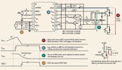
ACPL-339J DESAT pin monitors the IGBT’s collector-emitter voltage (VCE) during normal operation. If a short circuit occurs, high current flows through the IGBT causing it to come out of saturation into a DESAT mode. This causes the IGBT’s collector and emitter voltage to increase rapidly from a saturation voltage of 2 V. Once it crosses the ACPL-339J’s threshold of 8 V, a short circuit fault is registered and soft shutdown is triggered. To achieve “soft” shut down the optocoupler’s VGMOS pin turns on an external transistor to slowly discharge the IGBT gate. You can adjust the rate of the soft shutdown by choosing the characteristics of the external transistor and resistor value to minimize the IGBT overshoot. And, the DESAT operation completes by reporting the FAULT through a built-in isolated feedback path to the controller. Fig. 2 shows the step-by-step operation of the DESAT detection during a short circuit event.
The DESAT fault detection circuitry must remain disabled for a short period following the turn-on of the IGBT to allow the collector voltage to fall below the DESAT threshold. This time period, called the nominal DESAT blanking time (TBLANK), which is:
TBLANK = CBLANK × VDESAT / ICHG (1)
Where:
ICHG = Internal DESAT charge current
VDESAT = DESAT voltage
CBLANK = External DESAT capacitor
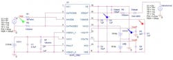
From datasheet specifications, VDESAT typical value is 8 V and ICHG is typically 250 µA. If 100 pF capacitor is used, then blanking time is 100 pF × 8 V / 250 µA = 3.2 µsec. You can scale the capacitance value slightly to adjust the blanking time, though a value smaller than 100pF is not recommended. This nominal blanking time also represents the longest time it will take for the ACPL-339J to respond to a DESAT fault condition. The simulation circuit in Fig. 3 demonstrates the DESAT detection operation.
The DESAT diode conducts forward current, allowing sensing of the IGBT’s saturated collector-to-emitter voltage, VCESAT, when the IGBT is on and to block high voltages when IGBT is off. During IGBT switching off and towards the end of the forward conduction of the DESAT diode, a reverse current flows for a short time. This reverse recovery effect prevents the diode from achieving its blocking capability until the mobile charge in the junction is depleted. During this time, there is commonly a very high dVCE/dt voltage ramp rate across the IGBT’s collector-to-emitter. This results in ICHARGE – CD-DESAT × dVCE/dt charging current, which will charge the blanking capacitor, CBLANK. To minimize this charging current and avoid false DESAT triggering, use fast recovery diodes.
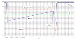
The freewheeling of flyback diodes connected across the IGBTs can have large instantaneous forward voltage transients that greatly exceed the nominal forward voltage of the diode. This may result in a large negative voltage spike on the DESAT pin which will draw substantial current out of the driver if protection is not used. To limit this current to levels that will not damage the driver IC, a 100 Ω resistor should be inserted in series with the DESAT diode. The added resistance will not alter the DESAT threshold or the DESAT blanking time. Fig. 4 shows that the nominal blanking time is accurately predicted in SPICE simulation, while Table 1 shows that the VGMOS and VOUTP delay time are tuned to datasheet typical specification.

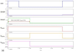
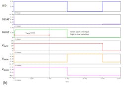
Once DESAT fault is detected and after TBLANK time, both VOUTP and VOUTN will turn off the respective external MP1 and MN1. The outputs will be muted for TMUTE time. All input LED signals will be ignored during the mute period, which allows the driver to completely soft shut down the IGBT. The fault is auto-reset upon the 1ms (typical) mute time (TMUTE) time out or upon LED input high to low transition, whichever happens later. In this way, there is a minimum time out but also the flexibility of lengthening the time out freely. Fig. 5a and 5b provide simulated illustrations of DESAT fault state timing diagram with LED turned off before and after TMUTE timeout, respectively.
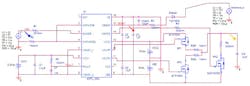
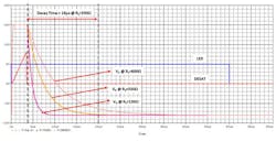
To illustrate an actual application where short circuit occurs, refer to the SPICE simulation circuit in Fig. 6. The SPICE model of the external MOS devices are also included to make the overall simulation more accurate. An IGBT SPICE model is not used in this simulation and is replaced by 10nF capacitor to emulate the gate capacitance of the IGBT. When a DESAT fault is detected, VGMOS switches from low to high, turning on an external MN2 pull down device. MN2 slowly discharges the IGBT gate at a decay rate corresponding to the RC constant of RS and input capacitance of IGBT, CIN. Based on a RS of 330 Ω and CIN of 10 nF, the entire soft shutdown will decay in 4.8 × 330 Ω × 10 nF = 15.8 µs. Soft shutdown prevents fast charges in the collector current that can cause damaging voltage spikes due to lead and wire inductance. The decay time of the IGBT soft shutdown can be changed by choosing different values for resistor RS, as shown in Fig. 7.
These details allow designers to understand the complex output logics and predict the performance of the overall circuits with ease by simulating the application circuits under different conditions. With DC and AC switching parameters precisely tuned to the datasheet typical specifications, it helps designers to choose the external components correctly. Thus, designers can use the ACPL-339J SPICE macro model with confidence for their complex circuit simulations and application requirements.
References
1. Tee Chun Keong, “Driving and Protecting IGBTs In Inverter Applications” Power Electronics, Aug 30, 2013
2. Jamshed Namdar Khan, “SPICE Circuit Simulations for the HCNR200 and HCNR201 Analog Optocouplers”, AV02-3334EN Application Note
3. “ACPL-339J Dual Output Gate Drive Optocoupler Interface with Integrated (VCE) DESAT Detection, FAULT and UVLO Status Feedback”, AV02-3784EN Datasheet, June 10, 2013
Comment About the Article
To join the conversation, and become an exclusive member of Electronic Design, create an account today!

Leaders relevant to this article: