Energy-Harvesting IC Pushes the Power-Management Envelope
The AEM10940 developed by e-peas (Liege, Belgium) is an energy-efficient power-management IC specifically intended to harvest dc power from photovoltaic (PV) cells, simultaneously store energy in a rechargeable device, and then supply two independent regulated voltages (Fig. 1). Typical energy-harvesting applications include industrial monitoring, geolocation, home automation, and wearables.
The AEM10940 boasts a number of features, such as:
• Ultra-low power boost converter (94% efficient)
• Voltage reference
• Power management
• LDO regulators
• Cold-start circuit
The power-management IC harvests the available input power up to 50 mW. It employs an ultra-low-power boost converter to charge a storage element. The boost converter operates with input voltages ranging from 100 mV to 2.5 V.
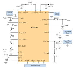
This power-management subsystem can charge a storage element (battery or supercapacitor, connected to the BATT pin) from an energy source (connected to SRC), which is often a miniaturized energy harvester (PV cell). The IC manages the transfer of energy from the source to any storage element through the boost converter, and from this storage element to the load through two embedded LDO regulators.
A 1.8-V LDO (LVOUT) can power up to a 10-mA load, typically for a microcontroller. A high-voltage LDO (HVOUT), configurable between 2.2 and 4.2 V, can sustain up to an 80-mA load and usually handles tasks that involve powering an application based on BLE, Zigbee, SIGFOX, LoRa, etc.
Dedicated status pins (HVRDY and LVRDY) report the status of the LDO regulators. An additional status (LOBATT) reports when the subsystem is about to shut down due to an input energy shortage.
Figure 2 presents a simplified view of the AEM10940’s internal power path. The energy source is connected to SRC and delivers power to the subsystem at optimal levels of voltage (VSRC) and current (ISRC), the so-called Maximum Power Point (MPP). Periodically, the MPP control circuit disconnects the source from the BUFSRC pin with the transistor Q1 in order to measure the open-circuit voltage of the harvester. Capacitor CSRC decouples BUFSRC, which smooths the voltage against the current pulses induced by the boost converter.
The power path contains two regulated switching converters: boost converter and buck converter. The boost (or step-up) converter raises the voltage available at BUFSRC to a level suitable to charge the storage element, in the range 2.2 to 4.75 V, according to the selected operating mode. This voltage (VBOOST) is available at the BOOST pin. The switching transistors of the boost converter are Q3 and Q4, with the switching node available externally at SWBOOST. The reactive power components are the external inductor (LBOOST) and capacitor (CBOOST).
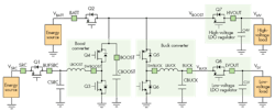
The storage element is connected to the BATT pin, at a voltage VBATT. This node links to BOOST through the transistor Q2. In normal operation, the transistor effectively shorts the battery to the BOOST node (VBATT = VBOOST). When energy harvesting occurs, the boost converter delivers a current shared between the battery and the loads. If there’s a risk of overdischarge, Q2 switches off to disconnect the battery.
The buck (or step-down) converter lowers the voltage from VBOOST to a constant value (VBUCK) of 2.2 V. This voltage is available at the BUCK pin. The switching transistors of the buck converter are Q5 and Q6, with the switching node available externally at SWBUCK. The reactive power components are the external inductor (LBUCK) and capacitor (CBUCK).
VBOOST feeds the high-voltage LDO regulator that powers its load through the HVOUT pin.
This regulator delivers a clean voltage (VHV) adjustable between 2.2 V and VBATT—0.3 V and a maximum of 80 mA. The output of the regulator’s series pass transistor (Q7) is decoupled by external capacitor CHV.
VBUCK feeds the low-voltage LDO regulator that powers its load through the LVOUT pin. This regulator delivers a clean fixed voltage (VLV) of 1.8 V at 10 mA, maximum. The output of its series pass transistor (Q8) is decoupled by external capacitor CLV.
Cold Start
Figure 3 describes the operating regions of the AEM10940. A unique cold-start circuit can start operating with empty storage elements at an input voltage as low as 380 mV and an input power of just 11 μW. Operation starts in the Cold Start region, a state where all nodes are deeply discharged. As soon as a small amount of energy becomes available at the source pin, the Cold Start mechanism raises VBOOST to 2 V.
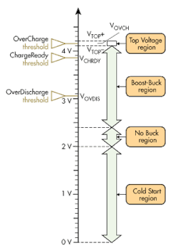
At that stage, the boost regulator switches on and continues the process of charging the BOOST node with the energy delivered by the source. However, the buck regulator is not yet activated, but its transistor Q5 is on, which also allows for charging of the BUCK node through inductor LBUCK. This occurs in the No Buck region.
When both VBOOST and VBUCK reach 2.4 V, the buck regulator switches on, and the device enters the Boost-Buck region. Under control of the charge manager, transistor Q2 connects the battery to the BOOST node, prompting normal operating mode. Both buck and boost switching converters are now active.
In the built-in configuration mode, four combinations of voltage levels are hardwired and selected through the CFG0, CFG1, and CFG2 configuration pins, covering most applications. You can set four voltage levels to suit the application’s requirements:
• OverDischarge threshold
• ChargeReady threshold
• OverCharge threshold
• HVOUT
Customizing the threshold levels involves a resistor ladder (R1 to R4) connected to BOOST and feeding SET_OVCH, SET_CHRDY, and SET_OVDIS (Fig. 1, again). Customizing the voltage at HVOUT involves two resistors (R5 and R6) feeding FB_HV, the feedback node of the high voltage LDO regulator, as shown in Fig. 1.
As long as this normal operating mode is active, VBOOST reflects VBATT. The three voltage thresholds control a charge-management state machine. If VBOOST decreases below the OverDischarge level, it causes a shutdown. When VBOOST reaches the ChargeReady level, it activates the two LDO regulators. If VBOOST increases above the OverCharge level, it triggers a mechanism to prevent further voltage increases, as indicated by the Top Voltage region.
In addition, a dedicated configuration pin (SELMPP) is available for selection of the MPP tracking mode best suited to the type of energy harvester in use.
Overvoltage Protection
To prevent damage to the battery and internal circuitry when the charge is complete, the charge manager maintains VBOOST between VTOP+ and VTOP–. This small voltage range comes from a hysteresis assigned to the OverCharge threshold. It is indicated as a toggling between the following two states.
In “Normal Operation,” the boost converter is enabled and feeds the BOOST node, charging the battery. In “Top Voltage Operation,” the converter is disabled, and the voltage drops due to the load consumption.
Overdischarge Protection
Deep discharge can damage the battery and cause the high-voltage LDO regulator to malfunction. As a result, the charge manager takes an emergency action if VBOOST drops below VOVDIS by transitioning from “Normal Operation” to “Entering Shutdown.” Both LDO regulators remain enabled. This allows a microcontroller powered by LVOUT to be interrupted by the low-to-high transition of the status output LOBATT, and take all appropriate actions before power shutdown.
An internal timer counts down a delay of at least 400 ms before determining a state transition to “Unloaded Voltage Rising,” where the battery is disconnected and the LDO regulators are disabled. At this point, the BOOST node is completely unloaded, which gives the boost converter the opportunity to collect energy from the source and restore the required voltage.
The boost converter remains activated except during cold start and in the “Top Voltage Operation” condition. Regulation of the boost converter involves a reference voltage (VMPP) issued by the MPP internal module.
To deliver maximum power, the energy source (PV cell) should be operated at a precise point in its I/V curve, which is its Maximum Power Point, or MPP.
VMPP is the voltage level of the MPP, and depends on the current level of PV-cell illumination. The MPP module evaluates VMPP as a given fraction of VOC, the open-circuit voltage of the source. By temporarily disconnecting the source with Q1, the MPP module gets and maintains its knowledge of VMPP. This sampling occurs regularly.
Except during this sampling process, the voltage across the source (VSRC) is continuously compared to VMPP. When VSRC exceeds VMPP by 25 mV, the boost converter switches on, extracting electrical charge from the source and lowering its voltage. When VSRC falls below VMPP by 25 mV, the boost converter switches off, allowing the harvester to accumulate new electrical charges into CSRC and ultimately restore its voltage.
In this manner, the boost converter regulates its input voltage so that the electrical current (or flow of electrical charge) entering the boost converter yields the best power transfer from the harvester in any ambient condition.
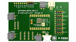
Evaluation Board
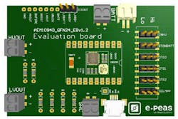
An evaluation board includes all of the components required to operate an AEM10940 (Fig. 4). The circuit board provides easy connections to the energy source and battery, as well as to LVOUT and HVOUT. It also features all of the configuration items to set the device in any mode. Control and status pins are available on standard pin headers, enabling wiring for various applications and evaluation of system performance.

About the Author

Sam Davis
Sam Davis was the editor-in-chief of Power Electronics Technology magazine and website that is now part of Electronic Design. He has 18 years experience in electronic engineering design and management, six years in public relations and 25 years as a trade press editor. He holds a BSEE from Case-Western Reserve University, and did graduate work at the same school and UCLA. Sam was the editor for PCIM, the predecessor to Power Electronics Technology, from 1984 to 2004. His engineering experience includes circuit and system design for Litton Systems, Bunker-Ramo, Rocketdyne, and Clevite Corporation.. Design tasks included analog circuits, display systems, power supplies, underwater ordnance systems, and test systems. He also served as a program manager for a Litton Systems Navy program.
Sam is the author of Computer Data Displays, a book published by Prentice-Hall in the U.S. and Japan in 1969. He is also a recipient of the Jesse Neal Award for trade press editorial excellence, and has one patent for naval ship construction that simplifies electronic system integration.
You can also check out his Power Electronics blog.
Comment About the Article
To join the conversation, and become an exclusive member of Electronic Design, create an account today!

Leaders relevant to this article: