Packaged in a multi-chip module, the IR3847 is a new member of International Rectifier’s SupIRBuck® family that is a Point-of-Load (POL) voltage regulator, providing:
•Efficiency up to 96%
•A temperature rise at 25 A as low as 50 °C
•Operation at 25 A without a heat sink
•20% less PCB size compared with other integrated solutions
•70% less PCB size compared with a discrete power MOSFETs and controller IC
•A 25 A POL regulator with a 168 mm2 footprint
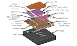
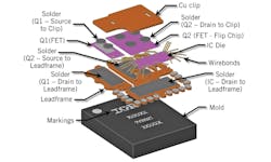
The ability to operate at up to 25A is made possible by a new, thermally enhanced 5 x 6 mm PQFN (Power Quad Flat No-Lead) package using a copper clip, as shown in Fig. 1.
Fig. 1. Fabrication of the IR3847 MCM involves four layers of components, topped by a copper clip for thermal enhancement.
Fig. 2. The MOSFETs and control IC are soldered into the package. Heat generated at the source of the flipped chip synchronous MOSFET goes directly to the PCB ground plane using vias, rather than going through the die first.
The cross section of the PQFN package in Fig. 2 shows that heat goes from the source of the synchronous MOSFET directly to the IR3847’s exposed pad and then onto a multilayer PCB’s vias that interface with its power ground plane. The sidebar, “IR3847 Features” summarizes the chip’s features, while the sidebar “IC Packaging Holds the Key to Product Improvements” discusses the part’s packaging attributes.
REGULATOR OPERATION
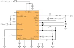
Fig. 3 shows a 12 V to 1.2 V POL using the IR3847’s internal low dropout (LDO) regulator as a bias supply. The LDO connects to the VCC pin, allowing operation with single supply. This bias voltage varies according to load conditions to optimize efficiency. If the output load current is less than half the peak-to-peak inductor current, the IR3847 provides 4.4 V for its internal gate drive to minimize switching losses, otherwise it supplies 6.8 V to minimize conduction losses.
Fig. 3. Application of the IR3847 as a 12 V to 1.2 V, 25 A POL using the internal LDO.
PWM voltage mode control with external compensation provides good noise immunity and maximum flexibility for selecting component values. You can program the switching frequency between 300 kHz and 1500 kHz by connecting an external resistor from the Rt/Sync pin to AGND. Two external resistors from the FB pin set the regulated output voltage from 0.6 V to 0.86 × PVIN (power stage input voltage).
A proprietary PWM circuit reduces jitter by 90% compared with standard solutions and cuts output voltage ripple by approximately 30%. This allows higher frequency/higher bandwidth operation that allows use of smaller size external capacitors and inductors. It also provides better transient response and requires fewer output capacitors.
This MCM utilizes the on-resistance of the low side synchronous MOSFET to sense output current. This enhances the regulator’s efficiency and reduces cost by eliminating the need for an external current sense resistor. The two integrated low RDS(ON) MOSFETs are optimized for high efficiency applications.
Body Braking provides improved response for step-down load transients that cause an overshoot in the output voltage and drive the Comp pin voltage down until it causes control saturation.. If that occurs, the IR3847 enters Body Braking mode, where the Sync MOSFET also turns OFF. Inductor current then decays by freewheeling through the body diode of the synchronous MOSFET. The MOSFET’s body diode forward voltage drop provides an additional voltage to speed the discharge of inductor current to its light load value.
Under-voltage lockout monitors the voltage at the VCC and Enable pins. This ensures that the MOSFET driver outputs remain off whenever either of these two signals drops below their set thresholds. Normal operation resumes once VCC and Enable rise above their thresholds. A POR (Power On Ready) signal asserts when these two signals reach their valid logic levels, which then initiates a soft start sequence.
The Enable input has a precise pre-set threshold monitored internally by an under-voltage lockout (UVLO) circuit. It prevents the IR3847 from turning on until the Enable pin voltage exceeds its pre-set threshold, typically 1.2 V.
Over Current Protection (OCP) senses the inductor current flowing through the synchronous MOSFET. Upon detecting over current, the regulator enters a hiccup mode. It will repeat the hiccup mode and attempt to recover until removal of the overload or short circuit. The OCP signal clears when the hiccup mode ends and then the regulator returns to its nominal output voltage using a soft start sequence.
The IR3847 continually monitors the output voltage via a dedicated sense pin (VSNS) that is an input to a window comparator. The dedicated pin is a robust solution to guarantee that the output voltage is monitored under all conditions. When the VSNS voltage is within the PGood comparator window threshold the PGood signal goes high, which indicates that output is in regulation. The open drain PGood pin must be pulled high with an external resistor.
Over-voltage protection (OVP) compares the voltage at VSNS to a pre-set over-voltage threshold. If VSNS exceeds the over-voltage threshold, a trip signal asserts after 2.5 µS (typical) delay. This immediately latches off the high side drive signal and sets the PGood flag low, which indicates the output voltage is out of regulation.
Thermal over-temperature protection (OTP) employs a trip threshold at 145°C junction temperature (typical). Exceeding this threshold causes thermal shutdown that turns off both MOSFETs and resets the internal soft start. Automatic restart initiates when the sensed temperature drops within the proper operating range, including a 20°C hysteresis in the thermal shutdown threshold.
As shown in Fig. 3, the RS+ and RS- pins provide remote sense capability when applied to the load. These pins connect to a differential amplifier with high speed, low input offset and low input bias current that ensures accurate voltage sensing and fast transient response in high current load applications.
An internal phase lock loop (PLL) enables synchronizing the internal oscillator to an external clock. This avoids sub-harmonic oscillations due to the beat frequency for embedded systems with multiple POL regulators. The external clock connects to the Rt/Sync pin.
LAYOUT
Layout is very important when designing high frequency switching regulators because it can affect noise pickup and cause a good design to perform with less than expected results. Connect the power components in the multilayer PCB’s top layer with wide, copper filled areas or polygons. It is usually desirable to use power planes and polygons for power distribution and heat dissipation.
Locate the inductor, input capacitors, output capacitors and the IR3847 as close as possible to each other. This helps to reduce any EMI radiated by the power traces due to their high switching currents. Place the input capacitor directly at the IR3847’s PVIN pin. And, keep the feedback components away from the inductor and other potential noise sources.
Use at least one layer of a multilayer PCB as a power ground plane and use the analog ground (AGND) as a reference for all required signals. Localize the high current path to a separate loop that does not interfere with the more sensitive analog control functions. The analog (AGND) and power (PGND) grounds must be connected together on the PC board at a single point.
The critical bypass components such as capacitors for PVIN, VIN and VCC should be close to their respective pins. Also, place the feedback resistors and compensation components close to the FB and Comp pins. Place all the compensation components over the analog ground plane in the top layer.
Based on thermal performance it is recommended to use at least a six-layer PCB. To effectively remove heat from the IR3847’s exposed pad, connect it to the multi-layer PCB’s power ground plane using vias.
DESIGN TOOLS
IR’s MyPower technology enables sophisticated online design support for the IR3847, which involves five steps:
•
Design Requirements Interview
Enter your design requirements, such as input and output voltage and current, switching frequency etc.
•Design Configuration
Automatically calculates optimum loop compensation and appropriate values for inductors and capacitors.
•Design Verification by Remote Simulation
It displays your design in an online schematic, which allows you to test your application in a virtual test bed. This allows AC, transient, and steady state analysis.
•PCB Layout and Thermal analysis
It allows easy drag and drop PCB layout editing, and state-of-the-art thermal analysis.
• Summary, Download, Design & More
Once the design has been verified, MyPower generates a Bill of Materials and a comprehensive design report including simulation results, schematic and design data.
embedded systems with multiple POL regulators. The external clock connects to the Rt/Sync pin.
LAYOUT
Layout is very important when designing high frequency switching regulators because it can affect noise pickup and cause a good design to perform with less than expected results. Connect the power components in the multilayer PCB’s top layer with wide, copper filled areas or polygons. It is usually desirable to use power planes and polygons for power distribution and heat dissipation.
Locate the inductor, input capacitors, output capacitors and the IR3847 as close as possible to each other. This helps to reduce any EMI radiated by the power traces due to their high switching currents. Place the input capacitor directly at the IR3847’s PVIN pin. And, keep the feedback components away from the inductor and other potential noise sources.
Use at least one layer of a multilayer PCB as a power ground plane and use the analog ground (AGND) as a reference for all required signals. Localize the high current path to a separate loop that does not interfere with the more sensitive analog control functions. The analog (AGND) and power (PGND) grounds must be connected together on the PC board at a single point.
The critical bypass components such as capacitors for PVIN, VIN and VCC should be close to their respective pins. Also, place the feedback resistors and compensation components close to the FB and Comp pins. Place all the compensation components over the analog ground plane in the top layer.
Based on thermal performance it is recommended to use at least a six-layer PCB. To effectively remove heat from the IR3847’s exposed pad, connect it to the multi-layer PCB’s power ground plane using vias.
DESIGN TOOLS
IR’s MyPower technology enables sophisticated online design support for the IR3847, which involves five steps:
•Design Requirements Interview
Enter your design requirements, such as input and output voltage and current, switching frequency etc.
•Design Configuration
Automatically calculates optimum loop compensation and appropriate values for inductors and capacitors.
•Design Verification by Remote Simulation
It displays your design in an online schematic, which allows you to test your application in a virtual test bed. This allows AC, transient, and steady state analysis.
•PCB Layout and Thermal analysis
It allows easy drag and drop PCB layout editing, and state-of-the-art thermal analysis.
• Summary, Download, Design & More
Once the design has been verified, MyPower generates a Bill of Materials and a comprehensive design report including simulation results, schematic and design data.
IR3847 FEATURES
• 5.0 to 21 V input range
• 0.6V to 0.86×PVIN output range
• Reference voltage available externally to enable margining
• 0.5% accuracy reference voltage
• Enhanced line/load regulation with feed-forward
• Programmable 300 kHz to 1.5 MHz switching frequency
• Internal digital soft-start
• Enable input with voltage monitoring capability
• Remote sense amplifier with true differential voltage sensing
• Thermally compensated current limit and hiccup mode over current protection (OCP)
• Internal LDO enhances light load efficiency
• Vp pin for voltage sequencing and tracking
• External synchronization with smooth clocking
• Dedicated output voltage sensing for Power Good indication and overvoltage protection (OVP)
• Enhanced pre-bias start up
• Body Braking improves transient response
• Integrated MOSFET drivers and bootstrap diode
• -40 °C to 125 °C operating junction temperature
• Thermal shut down for over-temperature protection (OTP)
• Post package trimmed rising edge dead-time
• Programmable Power Good output with tracking
• 5 mm x 6 mm PQFN
• Pb-Free (RoHS Compliant)
Sidebar: IC PACKAGING HOLDS THE KEY TO PRODUCT IMPROVEMENTS
After several decadesof relative obscurity, advancements in IC packaging technology are finally receiving chip manufacturers’ attention. Driving the changes in semiconductor packaging are user’s requirements for increased operating speed and higher functional density, which requires more sophisticated packaging. Plus, there are demands for the package to be smaller, thinner and less expensive, which imposes additional challenges.
One trend toward higher functional integration requires both a larger die size and reduced feature size. Another trend is for integration of multiple devices in a single package. These trends require improved design methods that can include electrical and thermo-mechanical modeling, attention to package reliability, and testing to ensure low defect levels.
These trends, along with emerging systems may require new IC packages to meet specific applications. In some applications, packaging technology will be a key differentiator for consumers and OEMs making purchasing decisions.
International Rectifier’s IR3847 is an example of more functional density and innovative packaging that produces a 25 A regulator MCM in a 5 x 6 mm PQFN package.
About the Author

Sam Davis
Sam Davis was the editor-in-chief of Power Electronics Technology magazine and website that is now part of Electronic Design. He has 18 years experience in electronic engineering design and management, six years in public relations and 25 years as a trade press editor. He holds a BSEE from Case-Western Reserve University, and did graduate work at the same school and UCLA. Sam was the editor for PCIM, the predecessor to Power Electronics Technology, from 1984 to 2004. His engineering experience includes circuit and system design for Litton Systems, Bunker-Ramo, Rocketdyne, and Clevite Corporation.. Design tasks included analog circuits, display systems, power supplies, underwater ordnance systems, and test systems. He also served as a program manager for a Litton Systems Navy program.
Sam is the author of Computer Data Displays, a book published by Prentice-Hall in the U.S. and Japan in 1969. He is also a recipient of the Jesse Neal Award for trade press editorial excellence, and has one patent for naval ship construction that simplifies electronic system integration.
You can also check out his Power Electronics blog.
Voice Your Opinion!
To join the conversation, and become an exclusive member of Electronic Design, create an account today!

Leaders relevant to this article:


