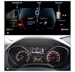
Automotive instrument clusters employ voltage-regulated subsystems that can include MCU, memory, and other ICs as well as stepper motors, communication interfaces, and displays. Fig. 1(a) and Fig. 1(b) are examples of current instrument clusters that present information by relying on subsystems that employ voltage-regulated power supplies. The recently-introduced MAX16993 power management IC (PMIC) from Maxim Integrated Products, Inc. has the potential to reduce the size, improve the efficiency, and minimize noise of future instrument cluster subsystems.
Related Articles
- Mixed-Signal ICs Manage Battery-Based Power Supplies
- Topology Key to Power Density in Isolated DC-DC Converters
- Chip-Scale DC-DC Converter Delivers High Efficiency
- High-Voltage Synchronous Regulators Address Industrial Power Dilemma
- Power Management Basics: Power Supply Characteristics
- Power Management Basics: Power Supply Fundamentals
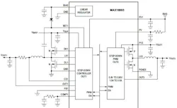
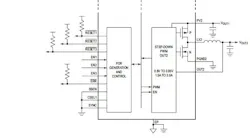
The MAX16993 is a 2.1 MHz, multichannel, dc-to-dc converter designed for automotive applications (Fig. 2). It reduces supply size by integrating three dc-to-dc converters in a single package. The device includes one high-voltage step-down controller (OUT1) designed to run directly from a car battery and two low-voltage step-down converters (OUT2 and OUT3) cascaded from OUT1. The IC is available in a 5 mm x 5 mm x 0.75 mm, 32-pin TQFN-EP and a 5 mm x 5 mm x 0.8 mm, side-wettable QFND-EP package. It is AEC-Q100 qualified and operates over the -40 °C to +125 °C automotive temperature range.
Buck1 controller (that produces OUT1) operates from a 3.5 V to 36 V input range, it can provide an output between 3.0 V and 5.5 V set at the factory or with external resistors. Buck1 drives two synchronous, external N-channel MOSFETs as the power switch elements. OUT1 current depends on the selected MOSFET, which can be up to 6 A. Key selection parameters for the external MOSFETs are:
● On-resistance (RDS(ON))
● Maximum drain-to-source voltage (VDS(MAX))
● Minimum threshold voltage (VTH(MIN))
● Total gate charge (QG)
● Reverse transfer capacitance (CRSS)
● Power dissipation
Both of OUT1’s N-channel MOSFETs must be logic-level types with guaranteed on-resistance specifications at VGS = 4.5 V when VOUT1 is set to 5 V, or VGS = 3 V when VOUT1 is set to 3.3 V. Conduction losses at minimum input voltage should not exceed MOSFET package thermal limits or violate the overall thermal budget. Also, ensure that the conduction losses plus switching losses at the maximum input voltage do not exceed package ratings or violate the overall thermal budget. In particular, check that the dV/dt caused by DH1 turning on does not pull up the DL1 gate through its drain-to-gate capacitance. This is the most frequent cause of cross-conduction problems.
Buck2 and Buck3 are high-efficiency, low-voltage converters with integrated, internal synchronous MOSFETs. They use a PWM current-mode control scheme operated at 2.1 MHz to optimize external component size and efficiency. These buck converters can be configured to deliver 1.5 A or 3.0 A per channel. They operate directly from OUT1 and have either fixed or resistor-programmable output voltages that range from 0.8 V to 3.95 V. Buck 2 and Buck 3 feature low on-resistance internal MOSFETs that contribute to high efficiency and smaller system cost and board space. Integration of the P-channel high-side MOSFET enables both channels to operate with 100% duty cycle when the input voltage falls to near the output voltage. They feature a programmable active timeout period that adds a fixed delay before the corresponding RESET_ can go high.
The two low-voltage converters (OUT2, and OUT3) run at a fixed frequency of 2.1 MHz. The high-voltage controller OUT1 has two frequency options that are pin selectable: 2.1 MHz or a lower frequency based on factory setting. Available factory-set frequencies are 1.05 MHz,
525 kHz, 420 kHz, or 350 kHz
To achieve quiet operation, the IC’s 2.1 MHz switching frequency avoids AM band noise and keeps the external inductors and capacitors physically small. The MAX16993 spread-spectrum mode reduces radiated EMI emissions. With spread spectrum enabled, the internal oscillator frequency varies between fSW and (fSW + 6%). The change in frequency has a sawtooth shape and a frequency of 4 kHz. This function does not apply to an externally applied oscillation frequency.
Factory-programmable synchronization I/O allows better noise immunity. When configured as an input, a logic-high on SYNC enables fixed-frequency, forced-PWM mode. Apply an external clock on the SYNC input to synchronize the internal oscillator to an external clock. The SYNC input accepts signal frequencies in the range of 1.7 MHz < fSYNC < 2.4 MHz. The external clock should have a duty cycle of 50%. A logic-low at the SYNC input enables the device to enter a low-power skip mode under light-load conditions.
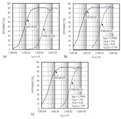
The synchronization input puts all the buck regulators either in skip mode or forced-PWM mode of operation. In the PWM mode, the regulator switches at a constant frequency with variable on-time. In the skip mode of operation, the regulator’s switching frequency is load dependent until the output load reaches a certain threshold. At higher load current, the switching frequency does not change and the operating mode is similar to the PWM mode. Skip mode helps improve efficiency in light-load applications by allowing the regulator to turn on the high-side switch only when the output voltage falls below a set threshold. As such, the regulator does not switch MOSFETs on and off as often as is the case in the PWM mode. Consequently, the gate charge and switching losses are much lower in skip mode.
Maximum efficiency of the three outputs is about 90% at 1A output as shown in Fig. 3(a), 3(b), and 3(c). The skip mode provides that efficiency at a lower load current than the PWM mode. Under no-load conditions, the quiescent current is only 30 µA with OUT1 enabled. This low quiescent current is significant because there are times when the instrument cluster is at no-load and in standby mode, and power dissipation is lower.
Circuit Protection
Fig. 2 shows the pin connections referred to below.
· Undervoltage-lockout activates if PV falls below the UVLO threshold (2.7 V, typ.). This turns off all three converters and set RESET_ outputs low.
· Buck converter overvoltage protection actuates if its output voltage threshold is exceeded. If this occurs, a discharge current is switched on at OUT1 and RESET1 asserts low.
· Soft-start time limits startup inrush current by forcing the output voltage to ramp up towards its regulation point.
· An open-drain, thermal-warning indicator (ESSR) asserts low if the junction temperature exceeds +145 °C (typ.).
· If the junction temperature exceeds +170 °C (typ.) an internal thermal sensor shuts down the three converters. The thermal sensor turns the device on again after the junction temperature cools by 30 °C (typ).
· Current limiting protects Buck 1 against short-circuit and overload conditions on the buck controller. Current-limit protection activates if the voltage across the current sense resistor (between CS1 and OUT1) increases above the 120 mV (typ.) current-limit threshold.
· The IC is also protected from load-dump transients up to 42 V.
PCB Layout
Careful PCB layout is critical to achieve low switching losses and clean, stable operation. Use a multilayer board whenever possible for better noise immunity and power dissipation. Follow these guidelines for good PCB layout:
1) Use a large contiguous copper plane under the device package. Ensure that all heat-dissipating components have adequate cooling.
2) Isolate the power components and high-current path from the sensitive analog circuitry. This is essential to prevent any noise coupling into the analog signals.
3) Keep the high-current paths short, especially at the ground terminals. This practice is essential for stable, jitter-free operation. The high-current path comprising of input capacitor, high-side FET, inductor, and the output capacitor should be as short as possible.
4) Keep the power traces and load connections short. This practice is essential for high efficiency. Use thick copper PCBs (2 oz vs. 1 oz) to enhance full-load efficiency.
5) The analog signal lines should be routed away from the high-frequency planes. This ensures integrity of sensitive signals feeding back into the device.
6) Use a single ground plane to reduce the chance of ground-potential differences. With a single ground plane, enough isolation between analog return signals and high-power signals must be maintained.
About the Author

Sam Davis
Sam Davis was the editor-in-chief of Power Electronics Technology magazine and website that is now part of Electronic Design. He has 18 years experience in electronic engineering design and management, six years in public relations and 25 years as a trade press editor. He holds a BSEE from Case-Western Reserve University, and did graduate work at the same school and UCLA. Sam was the editor for PCIM, the predecessor to Power Electronics Technology, from 1984 to 2004. His engineering experience includes circuit and system design for Litton Systems, Bunker-Ramo, Rocketdyne, and Clevite Corporation.. Design tasks included analog circuits, display systems, power supplies, underwater ordnance systems, and test systems. He also served as a program manager for a Litton Systems Navy program.
Sam is the author of Computer Data Displays, a book published by Prentice-Hall in the U.S. and Japan in 1969. He is also a recipient of the Jesse Neal Award for trade press editorial excellence, and has one patent for naval ship construction that simplifies electronic system integration.
You can also check out his Power Electronics blog.
Voice Your Opinion!
To join the conversation, and become an exclusive member of Electronic Design, create an account today!

Leaders relevant to this article:


