Space-Constrained Systems Call For Compatible Power Management Units
The trend toward smaller electronic systems has created a need for compatible size PMUs that supply dc power for the system. In addition to smaller size, these new PMUs should also duplicate characteristics of the previous generation of larger PMUs, such as:
· Input voltages that cover 5 V to 15 V.
· Output voltages that range from 0.6 V to 5 V
· Output current up to 4 A
· Multiple independent power sources that can be sequenced for different loads
· Limited power dissipation in a closed environment
· Design flexibility to customize a PMU’s features for a specific application.
· Fault handling for UVLO, OCP, OVP and OTP
· High efficiency (at least 90%)
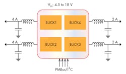
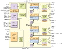
A PMU that meets the above characteristics is the TPS65400 from Texas Instruments. It consists of four buck-switching regulators (SW1, SW2, SW3, and SW4) with integrated power MOSFETs (Fig. 1). These switching power supplies will power high-current digital circuits such as processors, FPGAs, ASICs, memories, and digital I/Os. SW1 and SW2 support 4 A each, and SW3 and SW4 support 2 A each. Each regulator’s switching frequency is independently adjustable up to 2.2 MHz. Fig. 2 shows a simplified circuit diagram of the TPS65400.
This IC can support input voltages from 4.5 to 18 V, allowing it to be used in systems powered from a single 5 or 12 V intermediate power bus. High efficiency system power conversion is achieved by employing single-stage conversion. If the input supply is located more than a few inches from the TPS65400 converter, additional bulk capacitance may be required in addition to the ceramic bypass capacitors. A 47 μF tantalum capacitor is a typical choice.
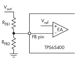
Regulators SW1 and SW2 can provide outputs of 0.6 V to 90%VIN and up to 4 A peak continuous current. SW3 and SW4 can provide outputs of 0.6 V to 90%VIN and up to 2 A peak continuous current. You can set output voltages through external resistor networks with all control and status info accessed through the PMBus-I2C bus. The output voltage of each switcher is set with a resistor divider from the buck output to FB pin and ground (Fig. 3). Use a 1% tolerance or better resistor to get maximum output voltage accuracy. You can set the output voltage according to:

Default VREF is 0.8 V, however, you can program it from 0.6 to 1.87 V using PMBus commands. As indicated in Equation (1), the VREF value will impact VOUT.
Output rails can supply higher currents by connecting SW1 and SW2 in parallel, or by connecting SW3 and SW4 in parallel. To configure this option, the COMP2 or COMP4 terminal must be tied to VDDA through a 4 kΩ resistor.
PMBus Controls
One way to customize a PMU’s features for a specific application is by using the PMBus-compatible I2C digital interface. The PMBus specification referenced by this section is PMBus Power System Management Protocol Specification Part I – General Requirements, Transport and Electrical Interface, Revision 1.2, dated 6 September 2010. Among the PMBus customization commands available in the TPS65400 are:
PMBus Runtime Control and Status
· Runtime Voltage Positioning Through Adjustment of VREF
· Enable and Disable of Each Switcher
· Fault and Status Monitoring
User-Configurable PMBus/I2C Options, Saved in EEPROM
· Switcher Turn-On and Turn-Off Sequencing
· Sequencing can be Based on Fixed Time Delays or PGOOD Dependence
· Initial Voltage Positioning Through VREF Configuration
· PWM Frequency Adjustment for Each Switcher
· Individual PWM Phase Alignment for Each Switcher to Minimize Ripple and Capacitor Size
· Adjustable Current Limit on Each Switcher Enables Size and Cost Optimization of Inductors
· Switcher Soft-Start Time
TPS65400 Pin Accessible Features Also Allow Customization:
· Adjustable Switcher VOUT With External Feedback Resistors
· Sequencing Control Through Precision Enable Pins for Each Switcher
· Resistor Adjustable PWM Switching Frequency from 275 kHz to 2.2 MHz
· Clock Sync Input and Clock Output
· Soft-Start Delay Using External Capacitor
· Current Sharing Between SW1 and SW2 and Between SW3 and SW4 for Higher Output Current, if Required
Regulator Sequencing
You can control the activation sequence for each switcher by using the individual enable pins (ENSWx) or by programming the sequence through the I2C bus into the onboard EEPROM (where x is 1, 2, 3, or 4: the switcher number). For external sequencing, either connect all the ENSWx enable pins to an external sequencing controller, or connect these pins to the PGOOD output. The Default PGOOD signal is the same for all switchers, however, it can be changed by a PMBus command. If all switchers are disabled, PGOOD is low. By default, tON_DELAY and tOFF_DELAY are both set to 0 ms, allowing complete flexibility of sequencing order and timing with the ENSWx pins. In addition, you can disable any switcher so that it is bypassed in the power-up sequence. For example, if the sequence is SW1-SW2-SW3-SW4, and SW2 is disabled, then SW3 will be powered up after SW1.
The TPS65400 can implement a soft-start function that minimizes discharge of the output when starting up. For digital soft-start you set soft-start time, tSS, with a PMBus command.
For analog soft-start you use buck regulator’s own soft-start pin, SSx (x is 1, 2, 3, or 4: the switcher number). A capacitor connected to the SSx pin sets the startup time. The SSx pin sources 5μA in charging the capacitor. In addition, you can refigure the SSx pin via the PMBus to display a PGOODx signal instead.
PWM Switching Frequency
The master clock frequency, FOSC, can be set by external resistor on the RCLOCK_SYNC terminal, or by synchronizing with an external clock. To sync to an external source, an AC-coupled signal should be applied to the terminal. A fixed resistor should still be connected to set a minimum frequency. The frequency of the input signal for synchronization should always be higher than the minimum frequency. If the internal PLL cannot synchronize, the switchers will fall back to the minimum frequency set by the resistor. The CLK_OUT terminal outputs the master clock, FOSC.
The PWM frequency of each switcher is determined by the master clock frequency and a PMBus command that sets one of the four divider ratios (1, 2, 4, or 8). Individual divider ratios allow designers to set the frequency of each switcher independently. For example, with a master clock FOSC of 1.1 MHz, SW1 and SW2 have a divider ratio of 4 for a 275-kHz PWM, and SW3 and SW4 have a divider ratio of 1 for a PWM frequency of 1.1 MHz. Select the divider ratio so that the PWM frequency stays within the range of 275 kHz to 2.2 MHz for whichever master clock frequency is set.
Fault Handling
Overvoltage protection (OVP), overcurrent protection (OCP), and undervoltage protection (UVP) are independently handled for each switcher. OVP or OCP faults that occur on one switcher do not affect the other outputs, exception for:
· A case where the current-sharing mode (ISHARE) is detected for a switcher with a fault, where both switchers in parallel have the same response to OVP or OCP.
· When using internal sequencing, in the case of faults occurring during the initial power-up sequence, all switchers are disabled for 500 ms, after which, the startup sequence is restarted.
A PMBus command sets the OCP. By default, the peak current for SW1 and SW2 is 6 A, and for SW3 and SW4 it is 3 A. When the current reaches that threshold, the unit immediately turns off the high-side MOSFET and keeps the low-side MOSFET off for the remainder of the switching cycle.
A UVLO (undervoltage lockout) function prevents startup when VIN is below 4V. In most applications, VIN and all of the power rails (PVIN1, PVIN2, PVIN3, and PVIN4) are tied to the same source so this single UVLO function is sufficient.
In cases where a single UVLO threshold is needed for all four switchers, but at a different level than 4 V, you can configure theTPS65400 for single-terminal enable where the ENSW1/ENSEQ terminal is used as a sequence enable terminal. Then, a resistor divider to the appropriate PVINx rail can be used to set a precise UVLO threshold that applies to all four switchers.
Feedback Compensation
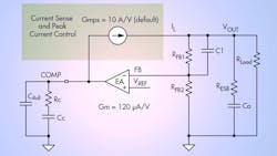
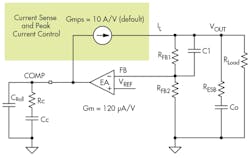
Fig. 4 shows the simplified compensation network for the TPS65400. A typical compensation circuit could be type II (RC and CC) to have a phase margin between 60° and 90°, or type III (RC, CC, and Cff) to improve the converter transient response. CRoll adds a high-frequency pole to attenuate high-frequency noise when needed. CRoll should be set to at least twice the crossover frequency to avoid interacting with the feedback compensation. It may also prevent noise coupling from other rails if there is possibility of cross coupling in between rails when layout is very compact.
Output Inductor Selection affects current ripple flowing in the inductor in CCM (continuous conduction mode):

Where:
ΔIL = Current ripple in the inductor
VOUT = Output voltage
VIN = Input voltage
L = Inductance in Henries
FSW = Switching frequency
Typically, the value of L is chosen to have the ripple current be 0.1× to 0.3× the full-load current. Choose the inductor so that the saturation current is higher than the maximum expected current plus half the current ripple at maximum operating temperature.
Also, the output capacitor needs to be properly sized to reduce voltage ripple due to the switching action and to reduce output voltage swings during transient load currents.
Layout Guidelines
Layout is critical in a high-current multi-channel DC-DC converters, like the TPS65400, so follow these guidelines:
· Place VOUT and SW on the top layer and an inner power plane for VIN· Also on the top layer, fit connections for the remaining pins of TPS65400 and a large top-side area filled with ground.
· Connect the top layer ground area to the internal ground layer or layers using vias at the input bypass capacitor, the output filter capacitor, and directly under the TPS65400 device to provide a thermal path from the power pad to ground.
· Tie the AGND pin directly to the power pad under the IC.
· For operation at full-rated load, the top-side ground area together with the internal ground plane must provide adequate heat dissipating area.
· Several signal paths conduct fast-changing currents or voltages that can interact with stray inductance or parasitic capacitance to generate noise or degrade the power supplies' performance. To help eliminate these problems, bypass the VIN pin to ground with a low-ESR ceramic bypass capacitor with X5R or X7R dielectric.
· Take care to minimize the loop area formed by the bypass capacitor connections, the VIN pins, and the ground connections. Because the SW connection is the switching node, the output inductor should be located close to the SW pins, and the area of the PCB conductor minimized to prevent excessive capacitive coupling.
· The output filter capacitor ground should use the same power ground trace as the VIND input bypass capacitor. Try to minimize this conductor length while maintaining adequate width.
· The compensation should be as close as possible to the COMP pins. The COMP and ROSC pins are sensitive to noise so the components associated to these pins should be located as close as possible to the IC and routed with minimal lengths of trace.
· The VFB node is a high-impedance analog node which is easier to pick noise on board. Keep FB node trace as short as possible.
About the Author

Sam Davis
Sam Davis was the editor-in-chief of Power Electronics Technology magazine and website that is now part of Electronic Design. He has 18 years experience in electronic engineering design and management, six years in public relations and 25 years as a trade press editor. He holds a BSEE from Case-Western Reserve University, and did graduate work at the same school and UCLA. Sam was the editor for PCIM, the predecessor to Power Electronics Technology, from 1984 to 2004. His engineering experience includes circuit and system design for Litton Systems, Bunker-Ramo, Rocketdyne, and Clevite Corporation.. Design tasks included analog circuits, display systems, power supplies, underwater ordnance systems, and test systems. He also served as a program manager for a Litton Systems Navy program.
Sam is the author of Computer Data Displays, a book published by Prentice-Hall in the U.S. and Japan in 1969. He is also a recipient of the Jesse Neal Award for trade press editorial excellence, and has one patent for naval ship construction that simplifies electronic system integration.
You can also check out his Power Electronics blog.
Comment About the Article
To join the conversation, and become an exclusive member of Electronic Design, create an account today!

Leaders relevant to this article: