Synchronous Buck Controller Can Step-Down from 48 Vin to 1 Vout
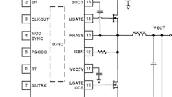
The ISL8117 from Intersil is a wide input-to-output voltage controller for external synchronous power MOSFETs (Fig.1). It is finding use in industrial and telecom applications where there is increasing interest in direct POL conversion, instead of using an intermediate bus. A higher-input voltage bus offers many advantages against lower-voltage 12V rails on the system board, including lower input current, less copper use, and lower loss in the system bus. Most important is the ability to remove one extra conversion stage wherever possible, hence improving total system cost and reliability. The key to providing this wide input/output characteristic is a function of the ISL8117’s pulse width modulator (PWM) and current control mode.
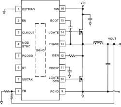
To understand how the ISL8117 operates we have to review how a PWM works in a switching converter. Figure 2 shows typical PWM outputs for different duty cycles. The PWM signal is applied to synchronous power MOSFETs whose output is rectified and filtered to obtain a dc output. The narrowest pulse width produces the lowest dc output voltage.
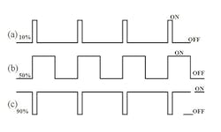
In high-voltage to low-voltage converters, a PWM’s ability to produce a minimum width output pulse depends on its current control mode. Using peak current mode control (Fig. 3), a gate voltage applied to the upper MOSFET (UFET) turns it on, but can produce output noise. Its attempt to produce a narrow PWM pulse width at a relatively high switching frequency affects the converter’s control loop response and results in a wider than expected pulse width and the wrong dc output voltage. This causes a switcher to employ pulse-skipping or burst-mode to correct for the DC output voltage. Unfortunately, these operating modes can cause excessive output ripple voltage.
Valley current mode control produces a more accurate minimum width output pulse by monitoring drain current when the lower MOSFET (LFET) is on, which avoids noisy UFET signals. Fig. 3 shows the valley current operating time related to the gate drive voltage. Adjustable adaptive slope compensation on a valley current mode provides stable compensation across a wide range of duty cycles. Plus, voltage feedforward improves PWM performance. These features provide the ISL8117 with the benefits of both a voltage mode and current mode modulator. The result is a switching converter that can provide a wide input-to-output voltage ratio, for example 48VIN and 1VOUT. Current sensing measures the voltage across the lower MOSFET’s RDS(ON).
This file type includes high resolution graphics and schematics when applicable.
Input-Output
The ISL8117 operates from input supplies ranging from 4.5V to 60V. The minimum input voltage (VIN(min) depends on:

Where:
Vd1 = Sum of the parasitic voltage drops in the inductor discharge path, including the lower FET, inductor and PC board.
Vd2 = Sum of the voltage drops in the charging path, including the upper FET, inductor and PC board resistances.
fSW = Switching frequency in kHz
VOUT = Output voltage
tOFF(min) = 308ns
The maximum input voltage (VIN(max) depends on:

Where:
tON(min) = 40ns in CCM and 60ns in DEM
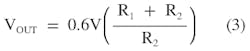
The ISL8117 has a 0.6V internal precision reference that determines the output voltage. This allows an output as low 0.6V and up to a level determined by the input voltage, maximum duty cycle and conversion efficiency. A resistive divider connected to the FB pin sets the output voltage, whose range is 0.6V to 54V.
The output voltage is:
Where:
VOUT = Output voltage
R1 = Top resistor of the feedback divider network (Fig. 1)
R2 = Bottom resistor connected from FB to ground (Fig. 1)
A Power-good pin (PGOOD) provides the status of the output voltage. PGOOD goes true (open drain) 1.1 ms after the FB pin is within ±11% of the reference voltage. There is no extra delay when the PGOOD pin is pulled low.
Switching Frequency
A resistor from the RT pin to GND sets the switching frequency from 100kHz to 2MHz. The choice of switching frequency is a trade-off between efficiency and component size. Low switching frequency improves efficiency by reducing MOSFET switching loss. To meet the output ripple and load transient requirements, however, operation at a low switching frequency requires larger size inductance and output capacitance.
A higher switching frequency allows small physical size inductance and capacitors in the output voltage filter, but causes higher-power MOSFET losses. There are two loss components: conduction and switching loss. These losses are distributed between the upper and lower MOSFETs. Conduction losses are the main component of power dissipation for the lower MOSFET. Only the upper MOSFET has significant switching losses, because the lower device turns on and off near zero voltage.
Using the MOD/SYNC pin, you can synchronize the ISL8117 to an external clock or the CLKOUT pin of another ISL8117. Connecting the MOD/SYNC pin to the CLKOUT pin of another ISL8117 synchronizes the two controllers.
At very light loads with MOD/SYNC tied to VCC5V, the converter goes into diode emulation and triggers pulse skipping. In this mode, the upper MOSFET remains off until the output voltage drops to the point the error amplifier output goes above the pulse skipping mode threshold. The minimum tON in the pulse skipping mode is 60ns.
Setting the EN pin high enables the controller and setting it low disables it. When the EN pin voltage is higher than 1.3V, the controller is enabled to initial its internal circuit. After the VCC5V pin reaches the UVLO threshold, soft-start circuitry becomes active. Soft-start time is set by the value of the soft-start capacitor. The internal 2μA charge current begins charging up the soft-start capacitor connected from the SS/TRK pin to GND. The output voltage thus rises from 0V to regulation as SS/TRK rises from 0V to 0.6V. Charging of the soft-start capacitor continues until the voltage on the SS/TRK pin reaches 3V. Adjusting the soft-start time controls inrush current during start-up.
Gate Drivers
Gate control logic translates the PWM signal into gate drive signals providing amplification, level shifting, and shoot-through protection. The gate driver helps optimize IC performance over a wide range of operational conditions. MOSFET switching times can vary dramatically from one type to another and with input voltage, so the gate control logic provides adaptive dead time by monitoring real gate waveforms of both the upper and the lower MOSFETs.
The low-side and high-side gate drivers provide a 2A peak sink and source current, which is adequate for some loads and eliminates the need for external power MOSFETs. Higher output currents require the synchronous power MOSFETs. Gate-drive voltage for the upper N-Channel MOSFET is generated by a flying capacitor boot circuit. A boot capacitor connected from the BOOT pin to the PHASE node provides power to the high-side MOSFET driver. To limit the IC’s peak current, place an external resistor between the BOOT pin and the boot capacitor. This small series resistor also damps any oscillations caused by the resonant tank of the parasitic inductances in the traces of the board and the MOSFET’s input capacitance.
The ISL8117 incorporates an adaptive dead time algorithm on the synchronous buck PWM controller that optimizes operation with varying MOSFET conditions. This algorithm provides approximately 16ns dead time between the switching of the upper and lower MOSFETs. This dead time is adaptive and allows operation with different MOSFETs without having to externally adjust the dead time using a resistor or capacitor.
External Components
There are three sets of critical components in a dc/dc converter using the ISL8117: the controller, the switching power components, and the small signal components. The switching power components are the most critical from a layout point of view because they switch a large amount of energy so they tend to generate a large amount of noise. The critical small signal components are those connected to sensitive nodes or those supplying critical bias currents. A multilayer printed circuit board is recommended.
Use logic-level MOSFETs for optimum efficiency given the potentially wide input voltage range and output power requirement. Two N-Channel MOSFETs are used in the external synchronous-rectified buck converters. These MOSFETs should be selected based upon RDS(ON), gate supply requirements, and thermal management considerations.
The PWM controller requires an output inductor that meets the output voltage ripple requirements. The inductor value determines the converter’s ripple current and the ripple voltage, which is a function of the ripple current and the output capacitor(s) ESR.
Important parameters for the input capacitor(s) are their voltage and RMS current ratings. For reliable operation, choose input capacitors with voltage and current ratings above the maximum input voltage and the largest RMS current required by the circuit. Capacitor voltage rating should be at least 1.25x greater than the maximum input voltage; 1.5x is a conservative guideline.
Capacitors for each output should meet the dynamic regulation requirements including ripple voltage and load transients. Selection is dependent on the output inductor, so some inductor analysis is required to select the output capacitors.
Layout
For successful implementation of an ISL8117 based dc/dc converter, pay attention to the necessary layout requirements. Of special note is the ISL8117’s pin architecture, which has been designed in such a way that it can run on a bare minimum circuit for a basic buck convertor. All additional function/feature pins have default values and can be sorted by leaving them floating or by tying them to VCC or GND. All high-power pins and signal pins are placed on opposite sides and therefore reduce any chance of interference. Also, the ISL8117 pins are organized to avoid layout errors by avoiding trace overlaps. The ISL8117 switches at a very high frequency, so switching times are very short. At these switching frequencies, even the shortest trace has significant impedance. Also, the peak gate drive current rises significantly in a short time. Transition speed of the current from one device to another can cause voltage spikes across the interconnecting impedances and parasitic circuit elements. These voltage spikes could degrade efficiency, generate EMI, increase device overvoltage stress and ringing. Careful component selection and proper PC board layout minimizes the magnitude of these voltage spikes.
The ISL8117 offers programmable soft-start and enable functions along and a power-good indicator for ease of supply rail sequencing and other housekeeping requirements. In ideal situations, a complete power supply circuit can be designed with 13 external components and provide OV/OC/OT protections in a space conscious 16 lead 4 mm x 4mm QFN or easy to assemble 6.4 mm x 5mm 16 lead HTSSOP packages. Both packages use an EPAD to improve thermal dissipation and noise immunity.
To reduce the number of external components and to simplify the process of determining compensation components, the controller includes an internally compensated error amplifier. In addition, the ramp signal applied to the PWM comparator is proportional to the input voltage provided at the VIN pin. This keeps the modulator gain constant with varying input voltages. Plus a load current proportional signal is derived from the voltage drop across the lower MOSFET during the PWM time interval and is subtracted from the amplified error signal on the comparator input. This creates an internal current control loop. The resistor connected to the ISEN pin sets the gain in the current feedback loop.
Protection
The converter output is monitored and protected against conditions that impact its operation:
- Undervoltage lockout (UVLO) keeps the IC in a reset condition until a proper operating voltage is applied. It also shuts down the ISL8117 if the operating voltage drops below a predefined value.
- An over-temperature protection circuit shuts the IC down if die temperature reaches +160°C. Normal operation resumes when the die temperature drops below +145°C.
- Overvoltage is set at 121% of the nominal output voltage set by the feedback resistors. In the case of an overvoltage event, the IC attempts to bring the output voltage back into regulation by keeping the upper MOSFET turned off and the lower MOSFET turned on.
- Over-current protection (OCP): The lower MOSFET's RDS(ON) monitors converter current. The sensed voltage drop is compared with a threshold set by a resistor connected from the LGATE/OCS pin to ground during the initiation stage before soft-start. If an overcurrent is detected, the upper MOSFET remains off and the lower MOSFET remains on until the next cycle. When OCP is triggered, the SS/TRK pin is pulled to ground by an internal MOSFET for hiccup restart.
Pricing for the ISL8117 QFN package is $1.80 USD and the HTSSOP is $1.95 USD in 1k quantities. For more information, visit www.intersil.com/products/isl8117. Watch a video of the ISL8117 evaluation and demo boards.
About the Author

Sam Davis
Sam Davis was the editor-in-chief of Power Electronics Technology magazine and website that is now part of Electronic Design. He has 18 years experience in electronic engineering design and management, six years in public relations and 25 years as a trade press editor. He holds a BSEE from Case-Western Reserve University, and did graduate work at the same school and UCLA. Sam was the editor for PCIM, the predecessor to Power Electronics Technology, from 1984 to 2004. His engineering experience includes circuit and system design for Litton Systems, Bunker-Ramo, Rocketdyne, and Clevite Corporation.. Design tasks included analog circuits, display systems, power supplies, underwater ordnance systems, and test systems. He also served as a program manager for a Litton Systems Navy program.
Sam is the author of Computer Data Displays, a book published by Prentice-Hall in the U.S. and Japan in 1969. He is also a recipient of the Jesse Neal Award for trade press editorial excellence, and has one patent for naval ship construction that simplifies electronic system integration.
You can also check out his Power Electronics blog.
Comment About the Article
To join the conversation, and become an exclusive member of Electronic Design, create an account today!

Leaders relevant to this article: