Dual, Hybrid High Power Module Boosts Op Amp Up to 2A Output
Boosting the power handling capability of a small signal, general purpose op amp, the Apex PB63 is dual high-voltage, high-current booster amplifier that operates at a 1 MHz bandwidth amplifier with a 1000V/µs slew rate.
Placing the power booster within the feedback loop of an op amp provides a composite amplifier with the accuracy of the op amp and the extended output current capability of the booster. As shown in Fig. 1, the PB63 output stage utilizes complementary MOSFETs, providing symmetrical output impedance. The booster’s flexibility allows the choice of driver amplifier, current limit and supply voltage.
Fig. 2 is an inverting composite amplifier consisting of one-half of the PB63 and an op amp. Cascading two amplifiers within a feedback loop has advantages, but also requires careful consideration of several system parameters. The most important of these are gain, stability, slew rate, and diver output swing.
You can maximize stability by observing the following:
- Keep gain-bandwidth product of the driver op amp lower than the closed loop bandwidth of the booster.
- Use the lowest possible booster gain.
- Minimize phase shift within the loop.
A good compromise is to set total (composite) gain at least a factor of three times booster gain. Phase shift within the loop is minimized through use of loop compensation capacitor CF when required. Typical values are 5pF to 33pF. Stability is the most difficult to achieve in a configuration where op amp effective gain is unity (i.e.; total gain = booster gain ).
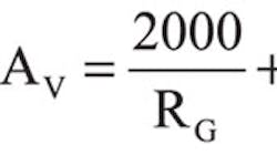
The gain of each section may be set independently by selecting a value for the gain setting resistor, RG, according to:
Where:
RG = Gain resistor in ohms
AV = Overall voltage gain of the composite amplifier
Recommended gain range is:
AV = 3V/V to AV = 25V/V
Slew rate of the composite amplifier is equal to the slew rate of the driver op amp times the booster gain, with a maxi¬mum value equal to the booster slew rate.
Maximum output voltage swing required from the driver op amp is equal to the maximum output swing from the booster divided by the booster gain. The offset voltage of the booster over temperature must be taken into ac¬count. Also, consider the effects of booster gain accuracy when calculating maximum available driver swing.
The composite amplifier should not be stressed beyond its absolute maximum supply voltage rating. It should be protected against any condition that may lead to its voltage stress level. Two common sources of overvoltage are the high energy pulses from an inductive load coupled back through flyback diodes into a high impedance supply and AC mains transients passing through a power supply that appear at the op amp supply pins.
Transients from the AC mains can be clamped using MOVs (Metal Oxide Varistors) or bipolar TransZorbs. Connect either of these devices across the inputs to the power supply to reduce transients before they reach the supply. You can add low pass filtering between the AC mains and the power supply to cut down on as much of the high frequency energy as possible. Inductors used in power supply filters will pass all high frequency energy. Capacitors used in the filter are usually electrolytics that have high ESR, so high frequency energy will not be attenuated fully and therefore will avoid the capacitor with little reduction.
Safe Operating Area (SOA)
Safe operating area (SOA) is an important parameter that determines the power handling capability of the PB63. Thermal considerations and current handling capabilities limit the SOA. The output stage is protected against transient flyback by the parasitic body diodes of the output stage MOSFETs. However, for protection against sustained high energy flyback use external fast-recovery diodes.
Fig. 3 shows the SOA curves for the PB63. The horizontal axis on the SOA curve, VS–VO, defines the voltage stress across the conducting output device. It does not define a supply voltage or total supply voltage or the output voltage. VS–VO is the magnitude of the differential voltage from the supply to the output across the transistor conducting current to the load. That is, if the amplifier is sourcing current, use (+VS)–VO, whereas if the amplifier is sinking current, use (–VS)–VO. The vertical axis represents the current that the amplifier is sourcing or sinking through its output pin.
The Safe Operating Area curves expose three limitations on the power handling capability of the amplifier:
1)Current handling ca pability. This horizontal line near the top of the SOA curve represents the limit on output current imposed by current density constraints in the power amplifier’s wire bonds, die junction area and thick film conductors.
2)A constant power line on the SOA curve is the power dissipation capability of the amplifier output stage. It is the product of output current on the vertical axis and VS–VO on the horizontal axis. For TC = 25°C, this line represents the maximum power dissipation capability of the amplifier at maximum junction temperature using an infinite heat sink. As case temperature increases, this constant power/thermal line moves toward the origin. The new constant power line can be determined from the Power Derating curves on the data sheet (Fig. 4). The case temperature is primarily a function of the heat sink used.
3)Second Breakdown is a phenomenon exhibited by bipolar transistors when they are simultaneously stressed with high collector-emitter voltage and high collector current. However, the PB63 employs MOSFET output power transistors, which do not have this second breakdown limitation.
Current limiting keeps the amplifier within its SOA. The PB63 has an adjustable current limit set with one external resistor for each half of the power booster amplifier. For optimum reliability the resistor value should be set as high as possible, with a maximum practical value of 30 Ω. You can disable the current limit by shorting the CL pin to the OUT pin. The current limit value for RLIM is:
Unidirectional zener diode transient suppressors are recommended as protection on the supply pins. The zeners clamp transients to voltages within the power supply rating and also clamp power supply reversals to ground. Whether the zeners are used or not, the system power supply should be evaluated for transient performance in¬cluding power-on overshoot and power-off polarity reversal as well as line regulation. Conditions that can cause open circuits or polarity reversals on either power supply rail should be avoided or protected against. Reversals or opens on the negative supply rail is known to induce input stage failure. Unidirectional transzorbs prevent this, and it is desirable that they be electrically and physically as close to the power amplifier as possible.
Inadequate power supply bypassing can lead to power amplifier circuit oscillations. Each supply pin should be bypassed to common with a low frequency bypass capacitance of 10µF/A of peak output current. Use tantalum capacitors, or computer-grade aluminum electrolytics for operating temperatures above 0°C.
In addition, a high frequency bypass 0.1µF to 1µF ceramic capacitor, should be added in parallel with the low frequency bypass capacitors from each supply rail to common. The ceramic capacitors must be mounted as close as possible (1/4-inch is good) to the supply pins.
The PB63 hybrid circuit utilizes a beryllia (BeO) substrate, thick film resistors, ceramic capacitors and semiconductor chips to maximize reliability, minimize size, and provide high performance. The circuit’s electrically isolated, 12-pin power SIP package handles operating temperatures of -25°C to 85°C.
npb63 Features:
- ±20 V to ±75 V input supply range
- Up to 2 A continuous output current
- Programmable gain
- 1000 V/μs typical slew rate
- Programmable output current limit
- 1 MHz typical power bandwidth
- 37 mA typical quiescent current (total, both channels)
Related Articles:
High-Side Current Monitor Uses Low-Voltage Amplifier
Current-Sense Amp Offers Four-Quadrant Operation
Back to Basics: Power Management Impacts All Electronic Systems
About the Author

Sam Davis
Sam Davis was the editor-in-chief of Power Electronics Technology magazine and website that is now part of Electronic Design. He has 18 years experience in electronic engineering design and management, six years in public relations and 25 years as a trade press editor. He holds a BSEE from Case-Western Reserve University, and did graduate work at the same school and UCLA. Sam was the editor for PCIM, the predecessor to Power Electronics Technology, from 1984 to 2004. His engineering experience includes circuit and system design for Litton Systems, Bunker-Ramo, Rocketdyne, and Clevite Corporation.. Design tasks included analog circuits, display systems, power supplies, underwater ordnance systems, and test systems. He also served as a program manager for a Litton Systems Navy program.
Sam is the author of Computer Data Displays, a book published by Prentice-Hall in the U.S. and Japan in 1969. He is also a recipient of the Jesse Neal Award for trade press editorial excellence, and has one patent for naval ship construction that simplifies electronic system integration.
You can also check out his Power Electronics blog.
Comment About the Article
To join the conversation, and become an exclusive member of Electronic Design, create an account today!

Leaders relevant to this article: