Layout Power Supply Boards to Minimize EMI: Part 1
With non-isolated topologies, one of the most basic topologies is the buck regulator. EMI starts off from high di/dt loops. The supply wire as well as the load wire should not have high AC current content. So, we can focus our analysis from the input capacitor, CIN, which should source all relevant AC currents to the output capacitor, COUT, where any AC currents end. To minimize EMI, we have to determine the “hot” loop in the circuit and reduce its impact.
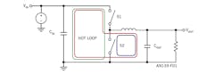
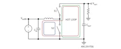
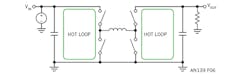
In the on cycle of a buck converter AC current follows through the red loop with S1 closed and S2 open (Fig. 1). During the off cycle, with S1 open and S2 closed, AC current follows through the blue loop. Both currents have a trapezoid shape. Designers often have difficulty grasping that the loop producing the highest EMI is not the red or the blue loop. Only in the green loop flows a fully switched AC current, switched from zero to IPEAK and back to zero. We refer to the green loop as a hot loop, because it has the highest AC and EMI energy.
To reduce EMI and improve functionality, you need to reduce the radiating effect of the green loop as much as possible. If we could reduce the PC-board area of the green loop to zero and buy an ideal input capacitor with zero impedance, the problem would be solved. But in the real world, we must find the optimal compromise.
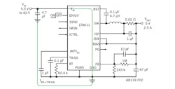
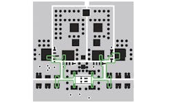
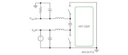
In the schematic in Fig. 2, the hot loop of the LT8611 buck converter is not easy to spot for layout purposes.
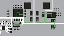
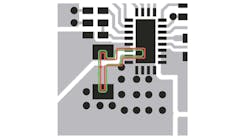
Fig. 3 shows an LT8611 buck converter demo board layout. Both switches are internal, so we only have to be concerned with the connection of the input capacitor. As shown Fig. 3, the green line is the hot loop in the top layer. AC current flows through the input capacitor and the switches in the part.
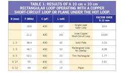
A copper short-circuit loop or plane under the hot loop improves the functional and EMI behavior of your circuit. Table 1 shows the result of an experiment with a 10 cm × 10 cm rectangular loop operating at 27MHz. The table indicates how much improvement a solid copper plane gives under the hot loop topside traces. The first line is no plane single layer. The inductance of a single-layer loop of 187 nH gets down to 13 nH in the case of only 0.13 mm insulation between the plane and loop traces. A solid plane on the next layer in a multilayer board (four layers or more) will have over 3× less inductance than a normal 1.5-mm, two-layer board with a solid bottom plane, and over 14× less over a single-layer board. A solid plane with minimum distance to the hot loop is one of the most effective ways to reduce EMI.
Where Does the Current Flow in the Plane?
The green top layer hot loop magnetic AC field produces eddy currents in the plane (Fig. 4).
Those eddy currents produce a mirror AC magnetic field, which is opposite the hot loop field (red trace). Both magnetic fields will cancel out. This works better the closer the mirror current is to the hot loop. Current is a round trip in the top layer. The most likely current path in the shield is the same round trip direct under the top layer. Both currents are almost the same. Since the plane current needs to be as high as the top trace current, it will produce as much voltage across the plane as is necessary to sustain the current. To the outside it will show up as GND bounce.
From an EMI perspective, small hot loops are best. The EMI from a power supply IC with integrated sync switches, optimized pinout and careful internal switch control will be less than a non-sync power supply IC with external Schottky diode. And, both will outperform a controller solution with external MOSFETs.
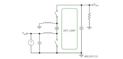
The boost circuit can be viewed in continuous mode as a buck circuit operating backwards. The hot loop is identified as the difference between the blue loop if S1 is closed and the red loop (Fig. 5) with S1 open and S2 closed.
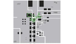
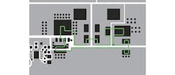
Fig. 6 shows the green hot loop of an LT3956 LED driver boost controller. The second layer is a solid GND plane. The main EMI emitter is the magnetic antenna the hot loop creates. The area of the hot loop and its inductance are tightly related. If you are comfortable thinking in inductance, try to decrease it as much as you can. If you are more comfortable in antenna design, reduce the effective area of the magnetic antenna. For near field purposes, inductance and magnetic antenna effectiveness are essentially the same.
The single inductor, four-switch buck-boost topology (Fig. 7) consists of a buck circuit followed by a boost circuit.
The layout will often be complicated by a common GND current shunt that belongs to both hot loops. An LTC3780 demo board (Fig. 8) shows an elegant solution splitting the sense resistor in two parallel ones.
A bit different drawing of a SEPIC circuit (Fig. 9) shows its hot loop.
Instead of an active MOSFET for the top switch, a diode is often used. The LT3757 demo board (Fig. 10) shows a good SEPIC layout. The green hot loop area is minimized and has a solid GND plane on the next layer.
Inverting, Flyback Topologies
The inverting topology (Fig. 11) is very similar to SEPIC, only the load has moved through the top switch and top inductor.
Layout is very similar, and demo boards can typically be modified from SEPIC to inverting provided the IC can also regulate on negative feedback voltage like LT3581, LT3757 etc.
The flyback topology (Fig. 12) uses separate windings on a transformer and there is only magnetic coupling between the primary and secondary windings. The current in the primary winding goes to zero at a relative high di/dt; only the energy stored in the leakage inductance and capacitance between windings and on the switch node slows that down. The primary and other transformer windings can be seen as fully switched current. We get two main hot loops as in the buck-boost case (Fig.7). To reduce EMI, in addition to close VIN decoupling for differential mode EMI, common mode chokes are used for the likely dominant common mode EMI in this topology.
For more information on reducing EMI, see the sidebar “Power Supply EMI Measurements.”
References
[1] http://www.conformity.com/past/0102reflections.html
[2] http://www.ece.msstate.edu/~donohoe/ece4990notes5.pdf
[3] http://de.wikipedia.org/wiki/Skin-Effekt 1.3.2011
[4] Rudnev, Dr. Valery I.; Heat Treating Progress; Oct. 2008
[5] Archambeault,Bruce R.; PCB Design for Real-World EMI Control; 2002
[6] Williams, Tim; EMC For Product Designers; Second Edition; 1996
[7] Johnson Howard, Graham, Martin; High Speed Digital Design A Handbook Of Black Magic; 1993
[8] Zhang, Henry J.; PCB Layout Considerations For Non-Isolated Switching Power Supplies; AN136; www.linear.com
[9] Ott, Henry W.; Electromagnetic Compatibility Engineering; Wiley; 2009
LT, LTC, LTM, Linear Technology, the Linear logo and LTspice are registered trademarks of Linear Technology Corporation. All other trademarks are the property of their respective owners.
Power Supply EMI Measurements
Most power supplies are relatively small compared to the wavelength of the relevant EMI frequencies they produce and are measured against. If prudently designed, in current power supply technology you will find most energy below 500MHz. EMI standards must be general and apply to equipment of variable size. Those can be in the order of the wavelength of interest. So they call for line conducted measurements up to 30 MHz and radiated measurements above 30 MHz. However reliable radiated measurements require large anechoic chambers. Their hourly prices are high and availability is scarce. Free field is too noisy, requires a large and difficult setup and is weather dependent.
For power supply optimization to work, a reasonable approach is to make line-conducted pre-compliance measurements up to the end of the spectrum required for radiated measurements. Since the power supply dimensions are still small against the wavelength of interest, we can assume that most energy will find its way through the VIN and VOUT wires, where we can measure them line conducted.
The setup is quite simple. We need a LISN (line impedance stabilizer network) or AN (artificial network), an input supply, a load and a measurement receiver.
The purpose of the LISN (AN) is to isolate the voltage source V1 from the power supply (or DUT device under test) VIN (VDUT+, VDUT).
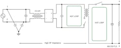
This is an example of a non-symmetric LISN often used in automotive applications (Fig. 13). Such a simple circuit can be made with L1 as air coil, or an inductor with losses can be used. Some standards specify different core types in series and a special winding scheme. However, the main purpose is to create a wideband high impedance against 50 Ω for L1.
Other than the wire length inside for C1, R1 and the VOUT_HF and L1 impedance, nothing limits the usable upper frequency range. So buy one or build your own. Resonances of L1 can be damped with a resistor over a part of L1 windings.
Any dedicated EMI receiver can be used, but a spectrum analyzer will usually do for pre-compliance work. Make sure that you use the AC-coupled input, since it provides a second barrier against blowing up your expensive mixer inside the analyzer.
From the EMI lab experts, you can expect a lengthy discussion about the required detection method from the used EMI standard, including peak, quasi peak, average with relative accurate time constants required for them. You can shortcut this discussion when your power supply operates fixed frequency in the load area of interest. At fixed frequency, only harmonics with a distance of the switching frequency can be created, a frequency comb. If the switching frequency is above the required resolution bandwidth (mostly 9 kHz up to 30 MHz and 120 kHz above 30 MHz), peak, quasi-peak and average methods will yield the same results, so you can use whatever your receiver provides. Some standards allow for the 9 kHz to use a 10 kHz bandwidth, and for 120 kHz, using a 100 kHz bandwidth. The error for a fixed frequency switching PSU, which operates well above 100 kHz, is not relevant for our pre-compliance task.
If your system includes a processor it can produce currents with large fluctuations with frequency contents well within the above resolution bandwidth.
Then, you need to refrain to the filter method your standard requires.
If you see components that are a fraction of the switching frequency or cannot be divided by integers to the switching frequency, check the switch node with an oscilloscope. In the time domain, you will likely see pulse skipping or subharmonic oscillation. Check the source for this behavior before proceeding further. Do not forget to unhook your scope probe because you get different results with the additional introduced probe antenna if you do EMI measurements with a probe attached.
Related Articles:
Pulse Withstanding Resistors Handle High Surges
Power Supply Redesign Raises EMC Issues
About the Author
Comment About the Article
To join the conversation, and become an exclusive member of Electronic Design, create an account today!

Leaders relevant to this article: