Layout Power Supply Boards to Minimize EMI - Part 3: EMI Basics
Electromagnetic far field impedance is about 377Ω = 120π or 29,9792458 × 4 × πΩ for the vacuum velocity of light. Any electromagnetic wave far enough from its source (rule of thumb >wavelength/2 × π) has a 377Ω relationship between its magnetic and electric field. Closer to the source, it can be a perfectly matched antenna, which transforms its input power source to the right 377Ω electromagnetic field. Or, there is significant mismatch and the antenna starts mainly as a magnetic field source or an electric field source.
The magnetic field source has a lower impedance of 377Ω. The electric field source has a higher than 377Ω impedance. The graph in Fig. 23
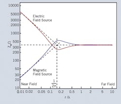
Fig. 23. Regardless if it starts as an electric or a magnetic field source, the electromagnetic field balances itself to its far field impedance.
shows that, regardless if it starts as an electric or a magnetic field source, the electromagnetic field balances itself to its far field impedance at a distance of:

where λ= Wavelength
Nonisolated switch mode power supply units have primarily magnetic field sources, since the impedances of the EMI-relevant loops with high di/dt are much lower than 377Ω unless you have very low current high voltage power supplies. So minimizing the AC magnetic fields on any nonisolated power supply unit will be the key to success.
Any isolated power supply unit will have AC loops with lower than 377 Ω, where the same magnetic field minimization as on non-isolated PSUs will be required. However, due to the very nature of isolation, we need higher impedances between the isolation barrier. On the isolation barrier, which is mostly done with a transformer, we try to get MΩ of isolation. On the isolation barrier, the electric AC field dominates and requires a different strategy. Here we try to get as low capacitive field coupling as possible. So we try to get as much distance as possible and to minimize the size of any conductive material.
Dipole Antenna Effect of the Hot Loop
When analyzing what the hot loop does, magnetic dipole antennas give a good clue.
The AC current flows around an area and creates the magnetic field part of a normal dipole antenna, as shown in Fig. 24.
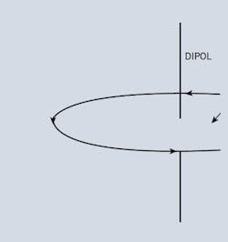
Fig. 24. The AC current flows around an area and creates the magnetic field part of a normal dipole antenna.
Magnetic antennas with loop diameters <<λhave very low radiation resistance. The range: µΩ to mΩ.

RR =
Radiation resistance in ohms
F = Area of magnetic loop
N =
Number of turns (= 1 in most layouts)
λ= Wavelength
with
practical layout loops

c = Speed of light ≈300000km/s
f = Frequency
The radiation resistance is low (mΩ) for typical dimensions of a PC-board power supply unit. Increasing the radiation resistance improves the matching and increases emitted radiation proportional to the radiation resistance. The parameter we can influence the most with layout is the area of the magnetic loop. The emitted radiation is proportional to the square of this area.
Skin Effect
To understand the effect of shielding, we need to dig a bit into the electromagnetic properties of the materials used. Electric current, whether or not it is tied to a conductor, will always flow on the path of least impedance. For higher frequencies, this will be the path of least inductance. This means the current will also flow on the path of its lowest losses. Electric conduction material minimizes any internal magnetic AC fields by creating eddy currents that oppose AC fields internal to the conducting material. Viewed from the outside, this looks like the skin effect, because the current density is forced to the outside of the conductor.
For another example, assume that the current, I, flows uniformly through a cylinder. This is a typical case for DC current.
If the current is DC, then it will look like the shape in Fig. 25.
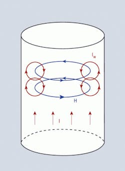
I is a constant, so the resulting H is constant and IW is zero. In the case that I has an AC content, which means there is di/dt, then the resulting magnetic field H changes. The changing magnetic field H creates induction voltage and since we are inside a conductor, the induction voltage creates an induced current IW, often referred to as eddy current. Eddy currents will create losses. If we assume that nature minimizes these losses, the only way to minimize this is to change the original uniform current distribution and let all current flow only at the surface of the cylinder. Now the magnetic field H is only at the surface of the cylinder. This way, the eddy currents IW are moved to the outside and the return path is cut off, omitting most of the eddy currents and its losses.
Skin Effect and Skin Depth
We can think of forces (Fig. 26) that move the current density to the outside of a conductor.
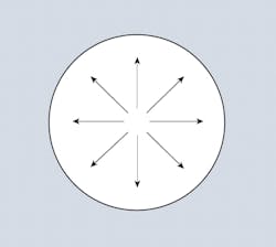
Fig. 26. Forces that move the current density to the outside of a conductor are called skin effect.
This is called skin effect. The wall thickness of a pipe, which would give the same resistance at DC as a full cylinder wire at AC, is called skin depth (Fig. 27).
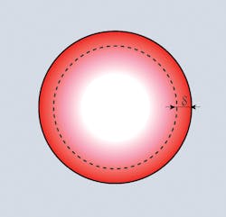
Fig. 27. Wall thickness of a pipe, which would give the same resistance at DC as a full cylinder wire at AC, is called skin depth.
Since the forces moving the current density to the outside are a result of the induc tion law, the skin depth goes down with rising frequency. Skin depth goes down with rising conductivity and goes down with increasing magnetic permeability.
For another example, assume we have a pipe wall conducting all the current on its surface, as shown in the large diameter in Fig. 28.
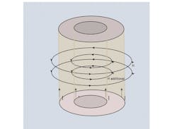
Fig. 28. Large diameter pipe wall conducting all the current on its surface. Total inductance of a given length of this wire is the complete volume integral of its magnetic field up to infinity or whatever physical size you assume for the universe.
Total inductance of a given length of this wire (1 meter or 1 foot whatever is most suitable) is the complete volume integral of its magnetic field up to infinity or whatever physical size you assume for the universe.
Now we shrink the pipe diameter to the smaller inner one shown in Fig. 28. The magnetic field is still the same as the larger pipe to infinity. However, we now have an additional magnetic field volume between the new small pipe and the prior larger pipe diameter. So the total integral of the magnetic field is now larger. This shows that the inductance is larger for a thinner conductor of a given length. Or, we can assume that the inductance increases as more of the current moves from the outer wall to the center of the wire. If we apply a voltage over both ends of the wire, the resulting current distribution is determined by the impedance. Since the inductance in the center is higher, most current density moves to the surface. The most extreme case of skin effect in conductors with zero resistance is shown in superconductors. There, quantum effects prevent all current from being bound to an outer layer of zero thickness. The thickness where most current is concentrated on superconductors is called London depth.
A graphof skin depth over frequency for some materials is shown in Fig. 29.
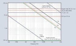
Fig. 29. Graph of skin depth over frequency for some materials.
We see that copper on typical PC-board material is affected by skin effect in the range of 5 MHz to 50 MHz. And, we see that even highly doped silicon at the thickness typically used on ICs is only affected in the terahertz region. Copper (Cu) and gold (Au) are close together. Materials with high
magnetic permeability, such as Fe-Ni, have low skin depth, even at audio frequencies. For this reason, material with high magnetic permeability is used to shield audio transformers.
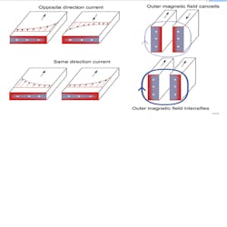
AC current through a good conductor will push current density to the outside. The current will flow where the impedance, dominated by inductance, is lowest. With regard to the impact of skin effect on layout and components, we can derive simple guidelines. Better is short and thick or wide. Reverse geometry capacitors have lower ESL because they are shorter and thicker. If we have opposite direction current, the same forces will attract the currents to each other (Fig. 30). This is called proximity effect.
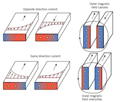
Fig. 30. Opposite direction current forces will attract the currents to each other, which is called proximity effect.
About the Author
Comment About the Article
To join the conversation, and become an exclusive member of Electronic Design, create an account today!

Leaders relevant to this article: