Chip-Embedded Packaging Contributes to New Performance Benchmark for DrMOS
In power supply design, reducing physical size while improving conversion efficiency is a sort of Holy Grail. The payoff for success is a potentially smaller overall system design, complemented by lower complexity and cost for thermal management. In DC-DC computing converters, this can either be achieved by increasing the switching frequency or by reducing the number of phases. Currently developed platforms use 600 kHz switching frequency and current per phase is approaching 40 A (TDC, thermal design current). Within the next four years, this is likely to increase up to 800 kHz and 60 A current per phase.
This places stringent requirements on power MOSFET products. Semiconductor technologies for power MOSFETs have improved significantly in the last years and still continue to improve. In the last ten years, area specific on-resistance (RDS(ON)) times chip area) has been reduced by approximately 75 percent, which means 25 percent chip area for the same on-resistance. Switching capacitances also have seen major enhancements. For example, the Figure of Merit FOMQg (RDS(ON) x Qg) improved by 75 percent. For discrete packages, major improvements from leaded SMD packages such as DPAPackaging Technology
In short, continuous improvements in semiconductor technologies will only realize full potential in the application environment with new packaging methods. We can derive the following requirements for the package technology:
• Low parasitic package resistance and inductance
• Low thermal package resistance to package bottom and top side
• Flexible integration of logic and power devices
• Flexible interconnect for small chip areas, with high current carrying capability
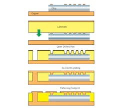
Infineon developed its Blade chip embedded packaging technology to meet these requirements. Blade doesn’t use standard interconnects like wire or clip bonding and doesn’t use the traditional molding process. Instead interconnects are done with galvanic processes and the die is protected by a laminate foil. The basic manufacturing process steps are (Fig.: 1):
Fig. 1. Blade packaging technology process steps: Diffusion soldering of chip on copper substrate, foil lamination, laser drilling of vias, Cu plating, patterning of structure.
1. Diffusion soldering of the chip on a copper leadframe
2. Lamination of an epoxy foil on thin chips (60µm)
3. Laser drilling of vias to chip and copper leadframe
4. Via filling by electro-plating of copper
5. Patterning of structure by a lithography/etching process
For integrated products with several routing layers some of the process steps have to be repeated. This approach yields clear advantages in comparison to traditional packaging.
• While interconnect technology is a limiting factor when working with continuously decreasing chip sizes, even the smallest chips can be connected with galvanic interconnects. These interconnects also can be optimized for highest current handling capability.
• With a high ratio between chip area and package area and with a minimum required distance between chips the package inductance and resistance can be minimized. This also results in a small package outline and enables lowest circuit loop inductance.
• Blade technology allows for flexible source and drain-down orientation of the chip within the package. This on the one hand minimizes current loops and on the other hand enables the quiet potential to be oriented into the direction of the cooling areas, e.g. low-side switch with source-down directly connected to PCB GND layers.
• Higher power density requires that the generated heat is transferred to the environment. Blade makes it possible to direct the heat flow specifically within the package, e.g. a low thermal resistance to the package bottom and top side enables double sided cooling.
• The flexible introduction of routing layers for integrated products offers an easy way to realize integrated products.
DrBlade
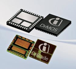
The first product of the upcoming Blade package family is DrBlade, an ultra-compact integrated MOSFET halfbridge with an integrated driver for DC-DC buck converter applications. The package outline is 5 x 5mm², which means 30 percent size reduction compared to the existing 6 x 6 mm² DrMOS (see Fig. 2).
Fig. 2. DrMOS 1.0 (top) and DrBlade (bottom).
With a thermal resistance to the package top-side for the low-side MOSFET of 1 K/W, compared to 20 K/W for the molded DrMOS package, DrBlade is the ideal choice for double sided cooling.
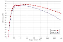
Measurement results of DrBlade1.0 in comparison to DrMOS in a 12V to 1.2V 4 phase DC-DC converter are shown in Fig. 3.
Fig. 3. Efficiency measurement of a 4-phase DC/DC converter (measurement conditions: VIN = 12V, VOUT = 1.2V, LOUT = 210 nH (DCR = 0.29 mΩ), fSWITCH 313 kHz, TAMBIENT = 25°C, 300 LFM, included losses: power stage, inductor and controller).
DrBlade shows 3 percent higher efficiency at 40 A output current, which means a reduction of the power losses of approximately 20 percent. Peak efficiency is 93.6 percent, which is 0.6 percent higher than for DrMOS.
Thermal measurements also show a significant improvement. For a system with 450 kHz switching frequency, 25°C ambient temperature, air flow of 100 lfm and no heat sink, DrBlade exhibits a 10°C lower device temperature, 65.9°C vs. 76.5°C, at a 40 A output current.
About the Author
Voice Your Opinion!
To join the conversation, and become an exclusive member of Electronic Design, create an account today!

Leaders relevant to this article:


