Combination VNA/FRAs Offer More Capability And Lower Cost
A frequency response analyzer (‘FRA’) is often used to measure gain and phase plots of control loops (Bode plots), filter responses and general frequency domain transfer functions. The FRA generally has a low impedance, high power oscillator and two, high impedance inputs. In many cases, the input ports are constructed using differential amplifiers. The FRA performs a frequency sweep and records the magnitude of the ratio of the two inputs and the phase shift between the two measurements. These are often plotted as magnitude (in dB) and linear phase as in a Bode plot, but can also be plotted in a Nyquist form. Since the FRA measures both magnitude and phase, it is technically a Vector Network Analyzer (‘VNA’).
An RF VNA (what we will refer to as a VNA) is quite different from an FRA. The VNA generally has two ports, each of which are maintained at a precise impedance. The most common impedance for a VNA is 50Ω, though there are also a fair number of 75Ω instruments supporting CATV requirements. The 50Ω ports are generally used to measure scatter parameters, or S parameters, as they are generally referred to. S parameters were developed to allow the precision port impedance to eliminate the errors caused by probing in higher frequency measurements. The VNA can measure the four transfer combinations referred to as S11, S21, S22 and S12. S11 is the reflection of the input port and S22 is the reflection of the output port. S21 is the gain from input to output and S12 is the gain from the output to the input.
|
|
Typical VNA |
Typical FRA |
|
Sensitivity |
uV |
mV |
|
Frequency range |
Hz to 10s of GHz |
mHz to 10s of MHz |
|
Dynamic range |
100-130dB |
>100dB |
|
Oscillator port |
Precision 50Ω (75Ω) |
2Ω |
|
Channel port |
Precision 50Ω (75Ω)/1MΩ |
1MΩ (often differential) |
|
Calibration |
Thru, Short-Open-Load |
Thru |
|
Native measurements |
impedance, gain and phase S11, S12, S21, S22 |
Gain and phase only |
|
Noise management |
Trace averaging, resolution bandwidth and graphically controlled oscillator |
Trace averaging, resolution bandwidth and graphically controlled oscillator |
Some instruments, such as the OMICRON Lab Bode 100 and the Agilent Technologies E5061B offer both the FRA features and the VNA features in a single instrument. This combination allows the measurement of scatter parameters, S11, S12 and S21 in addition to 1 port and 2 port impedance, including output impedance, as well as gain and phase plots.
Frequency Response Analyzer Functions
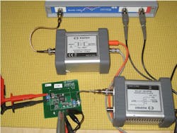
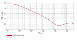
The 3uV sensitivity and >100dB dynamic range of the Bode 100 and slightly lower sensitivity and higher dynamic range for the E5061B are very helpful in making clean measurements of large magnitudes. A good example is the Analog Devices REF-03 PSRR measurement performed with the Bode 100 in Figure 1. This device offers 97dB low frequency PSRR and the measurement is very clean, so it is well below the noise floor of the instrument.
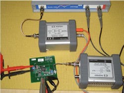
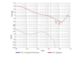
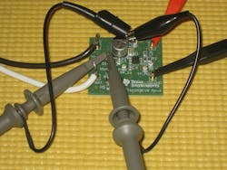
The FRA features also allow Bode plots to be measured on noisy switching converters such as the POL measurement shown in Figure 2.
S parameter Functions
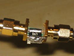
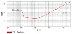
The S parameter measurement features of a VNA add many additional capabilities such as low noise measurements of very small magnitudes. The low noise aspect is important for PDN impedance measurements, critical for today’s FPGA designs. The ability to measure ultra-low impedances for PDN is demonstrated in the 250uΩ resistor measurement in Figure 3, performed with the addition of the Picotest J2180A preamplifier. This s parameter measurement reflects a -87dBm signal at port 2.
The S parameter capability includes Short, Open, Load and Thru calibrations, as well as short time delay and precise correction for the tolerance of the 50Ω terminator used in the calibration. The benefits of this complete calibration is that it can remove nearly all effects of the interconnecting probes and cables.
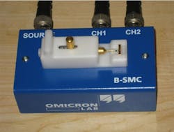
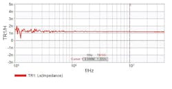
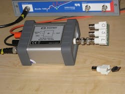
The short delay time calibration along with the OMICRON B-SMC impedance adapter allows the measurement of very low values of inductance such as ESL of ceramic capacitors. This capability is demonstrated in the measurement of a 0402 case size 1.2nH chip inductor shown in Figure 5.
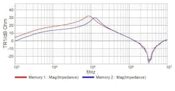
The s parameter capability also allows precise single port impedance measurements using a single cable. The addition of a Picotest J2130A DC Bias injector allows precise biasing of the junction and AC coupling to the Bode 100. The measurement is useful for, measuring the semiconductor parameters for SPICE models, measuring the output impedance of a low power opamp, voltage reference or voltage regulator, measuring passive resistors, capacitors and inductors or finding opens or shorts in a coaxial cables. The measurement in Figure 6 shows the output impedance of a LM285 voltage reference using a 0.1uF output capacitor and biased at 1mA (red) and 2mA (blue)
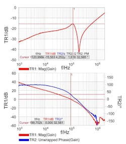
S parameters provide the basis for the non-invasive phase margin measurement from impedance [1][2][3], allowing the exact determination of phase margin in a 2nd order system from a single output impedance sweep. This is a unique capability currently offered only within the OMICRON Lab Bode Analyzer Suite software. An example of the non-invasive phase margin measurement is shown in Figure 7. This method allows the phase margin to be determined from devices that do not have access to the control loop. The cursor math determines the exact phase margin for 2nd order systems and can also determine the crossover frequency. The cursor frequency does not directly indicate the crossover frequency. Some examples where an FRA Bode plot cannot be performed while the VNA non-invasive can be applied are fixed voltage regulators, integrated POL regulators, voltage references, opamps and class D audio amplifiers to name a few.
These S parameter related features are not available in FRAs while they are available in most VNA’s including the OMICRON Lab Bode 100 and the Agilent Technologies E5061B. Application notes for both the OMICRON Lab Bode 100 and the Agilent Technologies E5061 are available for free at www.picotest.com/blog
References
- Ultra low impedance Measurements using 2 port measurements, Agilent Technologies 5989-5935EN
- Making sense of two-wire current-sense resistors, How2Power.com, July 2012
- Measuring ultra-low impedance and PDN’s, Electronic Design, June 15 2012
About the Author
Voice Your Opinion!
To join the conversation, and become an exclusive member of Electronic Design, create an account today!

Leaders relevant to this article:
