2014 Power Electronics Forecast Part 2: Semiconductors
The ever-increasing need for power-efficient electronics, coupled with advances in materials and production processes, is fueling a myriad of improvements in semiconductors. Several semiconductor industry executives viewed by Power Electronics gave their thoughts on what’s ahead for 2014:
Oleg Khaykin, President and CEO,
International Rectifier
In recent years, power management has risen rapidly up the design agenda and is now at the forefront of the engineer’s mind due to the ever-increasing demand for energy-efficient applications. Power levels and power density requirements continue to increase for many types of end equipment as systems are expected to deliver more functionality.
For example, in automotive, the electrification of the powertrain continues as increasing numbers of car manufacturers are adding Hybrid Electric Vehicles (HEV) and full Electric Vehicles (EV) to their platforms, driven in part to meet stringent emission regulations and targets. However, the mass adoption of EV and HEV depends largely on achieving cost, size and weight reduction and increased reliability of electric powertrain systems. Further progress towards achieving these performance and cost goals requires an innovative, comprehensive approach including the development of dedicated semiconductor devices and packaging concepts specifically for automobiles. Working closely with our automotive customers, International Rectifier has developed a complete, innovative, automotive high power semiconductor platform, called COOLiR™, that includes large IGBTs (CooliRIGBT™) and power MOSFETs (COOLiRFET™). We will continue to develop new families of IGBTs and MOSFETs using this new platform to meet the challenges of the automotive market.
I also believe that digital power management is entering a rapid adoption phase after being a niche technology for several years. Focus on energy efficient products over the next decade is expected to drive an expanding use of digital power management in applications such as DC-DC converters. IR offers end-to-end solutions that feature our high performance CHiL® digital ICs and PowIRstage® multi-phase devices for DC-DC applications including the high growth server market.
In the industrial and consumer segments, the use of permanent magnet variable-speed motors will continue to contribute to achieving greater energy savings and delivering increased performance. Integrated design platforms such as IR’s iMOTION™ platform which combine digital ICs and analog power components with control algorithms, development software and design tools simplify the development of industrial and home appliance applications using variable speed motors that can cut energy consumption by 60 percent.
At the same time, the availability of cost-effective, high quality, robust, high performance GaN-based power devices will enable truly innovative improvements in power electronic density, efficiencies and costs in the coming years across a wide range of applications/markets. From highest efficiency power supplies, to higher density, efficient permanent magnet-based motion control systems to lighter weight and more dense inverters for electrified vehicles, as well as next-generation integrated DC-DC power supplies for electronics, GaN-based power devices will revolutionize the industry
Dean Henderson, Director of Power Management, Infineon Technologies North America
Secular global trends, including growth in overall energy consumption and strong emphasis on efficiency goals, will continue to place a spotlight on the power semiconductor industry. In many ways, engineers in the power electronics field have never had more opportunity to have an impact on system designs, and they have never faced more pressure to innovate.
As always, the principal goals for power electronics design are to boost overall efficiency and achieve optimal system footprints. The contributions of semiconductor suppliers to realize these goals revolve around both device technology and access to expert support resources. For 2014, we will see constant improvement of operating characteristics through chip and module integration, implementation of system/sub-system level approaches to design, new technology and ongoing process refinement. The end result of these developments includes faster time-to-market, simplified design and reduced costs.
One example is in the just announced series of OptiMOS™ medium-voltage MOSFETs by Infineon Technologies. This 200/250 V product series with integrated fast body diode shows improved hard commutation ruggedness for enhanced reliability, as well as improved on-state resistance and Figure of Merit (FOM) reduction compared to alternatives.
>With improvements in device performance, packaging innovation at the chip and module level plays a large role. During 2014, Infineon will expand offerings of its Blade chip-embedded packaging for medium voltage supplies. This multichip package approach enables typical footprint reduction of 30 percent even while achieving the higher power density needed in computing and telecom systems. For high-voltage industrial power systems, customer demand will be met with an expanded portfolio of IGBT modules packaged with phase-change Thermal Interface Material that achieves a 74 percent reduction in thermal resistance compared to traditional thermal grease.
>
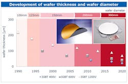
Continued technology and process refinement allow Infineon to drive engineering innovation by delivering best-in-class characteristics across the range of power semiconductor devices. With thin-wafer technology (IGBT) shown in Fig. 3 (make this Fig. 1), electrical and thermal resistance is optimized in the latest generation IGBTs and new SiC diode families (Fig. 4-make this Fig. 2). Substrate thicknesses range from 110 nm for SiC devices to nearly one-half that for the latest generation IGBT 5 devices, with a well-defined roadmap for further improvements. Concurrently, high volume MOSFET and soon IGBT product families will be produced on 300 mm wafers to support growing demand across consumer, commercial and industrial market segments.
As production experience contributes to steady growth in use of compound semiconductors such as SiC, we anticipate enablement of new applications and more segmentation in the markets now occupied by silicon devices. At the same time, new generation IGBT and SJ MOSFET generations will substantially increase efficiency and lower system cost in hundreds of application segments. The important role these types of devices play in achieving global goals for efficiency in all aspects of the electricity value chain and mobility applications provides a solid foundation for continued growth of opportunity for engineers working in power electronics design.
Alex Lidow, Efficient Power Conversion
Gallium nitride transistors designed as the successor to the aging power MOSFET have been widely available since early 2010. Since then several companies have entered the field with product in the 40 V to 600 V range with on resistance as low as a few milliohms. New applications that were out of reach for MOSFETs due to their limited switching speeds and relatively high capacitance, have emerged and will alter the entire landscape for power conversion.
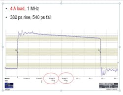
The fast switching speed of the GaN transistors translates into many benefits at the system level and is driving the first high-volume applications. In Fig. 6 (make this Fig. 3) is a 12 V switching waveform of a third-generation EPC8009 eGaN® FET from Efficient Power Conversion (EPC). Sub-nanosecond switching at high current and high voltage is possible for the first time! Such high-speed switching enables very short pulse-width that is critical in such applications as LiDAR (Light Detection And Ranging), RF Envelope Tracking, and wireless power transmission.
The ability to switch fast can quickly be negated by inefficient packaging due to parasitic package inductance. To avoid this problem, eGaN FETs use a chipscale format (Fig. 7-make this Fig. 4)) that essentially eliminates packaging altogether. This is not only the smallest possible form-factor, but it also enables minimum parasitic inductance and resistance in the entire power circuit. Older packages such as LFPAK and DirectFET® have too much internal inductance to operate efficiently in the megahertz switching range.
Even with efficient chipscale packages there is a need for a driver circuit that can keep up with the GaN transistor. In figure 1 the EPC8009 device is switching in a few hundred picoseconds, but the LM5113 driver IC is driving the gate at 1.2 ns. The transistor is switching twice as fast as the gate drive! Clearly there is a need for even faster gate drive ICs, and several are in development.
In the meantime there is work in progress at EPC to integrate several GaN transistors in a monolithic half bridge format. Look for product later in 2014. Even further integration of the driver circuit is possible, and products with multiple power transistors and their integrated driver circuits could be on the market as soon as 2015. Eliminating the parasitic inductance caused by using separate power devices and driver ICs enables a whole new level of switching performance that will result in higher resolution 3D LiDAR systems, higher efficiency RF transmission, and longer range, higher efficiency wireless power transmission.
Transistors in the 600 V range are already available from companies such as Transphorm and Panasonic in more traditional semiconductor packages. These products are setting new efficiency benchmarks in applications such as power factor correction and variable speed motor drives. GaN transistors do not suffer as much a performance loss with higher breakdown voltage compared with their silicon superjunction MOSFET and IGBT counterparts. This means smaller, lower cost transistors that also switch an order of magnitude faster.
GaN has been making rapid inroads into the territory once dominated by silicon. Entirely new applications are emerging, and older applications are setting new performance standards. As the volumes grow, EPC predicts that GaN transistors will actually cost less to manufacture than MOSFETs and IGBTs, leaving the design engineer as well as the purchasing manager an easy choice for the future.
Carl Blake, Transphorm Inc.
After overcoming persistent misconceptions in the industry, GaN (Gallium Nitride) power transistor technology has finally moved from the evaluation phase into the production phase. Transphorm’s announcement in March 2012 of being the first (and only) company to qualify 600V GaN HEMTs (high electron mobility transistors), played a key role in jumpstarting interest in power GaN. Now with the acquisition of the Fujitsu GaN team, Transphorm has both qualified products and high-volume product fab capacity to support the rapidly growing demand.
Transphorm's 600V HEMT products are geared to off-line power conversion or power inverters connected to the grid for solar and motor drives. Transphorm provides 600V transistors that outperform the best silicon 600V transistors in power conversion circuits (Fig. 9 –make this Fig. 5). In order to achieve even greater efficiency, the fixed losses of diodes must be eliminated. This is made possible by using Transphorm's GaN transistors in bridgeless PFC circuits in which existing silicon or SiC transistors simply will not work, due to the intrinsic body-drain diode reverse recovery.
Industry-wide, Transphorm has seen its GaN devices gaining acceptance. For example:
- Emerson published paper at PCIM China 2011 about using GaN in a totem pole PFC topology to achieve 99% efficiency
- Schneider presented a paper at PCIM 2013 evaluating the successful application of 600V transistors in UPS systems
- At the 2012 Solar conference, Japan, Yaskawa had a demo of a 4.5 kW solar inverter that used Transphorm's GaN HEMTs to achieve 40% lower power losses in a 40% smaller size, than what is possible by using silicon devices
- Transphorm was invited as the only GaN supplier to an internal seminar for Delta Electronics’ leading power designers, and the company is planning to implement GaN to achieve higher efficiency
Another milestone for Transphorm was acquiring Fujitsu's GaN power supplies businesses in Dec. 2013. As a result, Transphorm has added Fujitsu’s experts in GaN technology to expand Transphorm’s already very large team; gained exclusive access to a proven high-volume fab in Japan that is already producing GaN products; and acquired Fujitsu's proven customer base for GaN devices. Additionally, Transphorm adds Fujitsu's 200V e-mode devices to its portfolio of 600 V d-mode devices, which results in the broadest product offering of GaN devices in the market today.
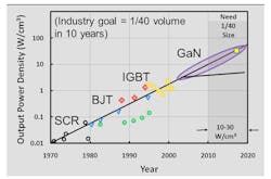
The primary long-term trend driving the adoption of GaN devices is the demand for higher efficiency and smaller-size power conversion products, as illustrated in Fig. 10 (make this Fig. 6). During the past 40 years, the focus has shifted back and forth between efficiency and smaller size. With the recent focus on efficiency, we believe the emphasis in 2014 will be for smaller size, and we will see the continuing trend of companies designing in high-voltage GaN in wider power ranges. As well-respected companies use GaN devices to significantly reduce system volume over what can be achieved with silicon products, the adoption of GaN devices will accelerate in the power conversion market.
Dave Freeman, Texas Instruments
Every New Year brings its own areas of focus applications and 2014 is no different. Two particular areas for 2014 where power management is important are wearable electronics and automotive electronics. There are certain themes that are timeless: high efficiency, high-power density and, of course, high value to price ratio.
Wearable electronics applications require multiple dimensions of operation. Managing the portable energy storage system without applying a significant drain is key. The wearable electronics designers spend a lot of effort to bring down their power requirement and do not want to have their efforts wasted by the power management system. This requires solutions that have quiescent current that is much below 1 uA, for example 100 s of nanoamps.
These systems also tend to have a peak-to-average power ratio. These ratios can be greater than 100. This drives the power management solution to have high efficiency over a wide load. In some cases the duty cycle product of the high-power mode and high power is about the same as product of the lower power duty cycle and the low-power requirement. So in this case, efficiency is important for both modes. Some wearable systems even have three or more modes of different power needs.
Practical wearable electronic appliances need optimization of all subsystems to meet the user expectations of long operating life and high functionality. We at TI focus on the total solution of minimizing the energy needs for the system, like processing and communication. These energy needs help our power management business to better target power requirements.
When it comes to automotive electronics, more and more consumer electronic devices are being added. This includes systems that provide improved automotive performance and safety, for example solid state lighting and electronic stability system. Additionally, multiple power rails are just starting to be integrated into our cars, such as 12 V and 48 V. The 48 V rail provides power for higher power devices. However, either rail needs a wide input DC/DC due to the variation in battery voltage due to load, temperature, and state of charge.
For example, the 12 V battery may have a range from 8 V to 17 V. But in order tolerate the transient range, the design may have to tolerate 6 V to 63 V. Another requirement is low-conductive electromagnetic interference (EMI). However, completely eliminating EMI is not practical. Therefore, DC/DC converters for automotive applications must be designed to minimize EMI production. At TI, we specifically design for EMI mitigation.
These are just examples of two areas where circuit designers will focus in 2014. There are many others like the “Internet of things,” the “Cloud,” and such. We will have a very enjoyable year providing integrated circuits to fuel the growth in these focus areas.
About the Author

Sam Davis
Sam Davis was the editor-in-chief of Power Electronics Technology magazine and website that is now part of Electronic Design. He has 18 years experience in electronic engineering design and management, six years in public relations and 25 years as a trade press editor. He holds a BSEE from Case-Western Reserve University, and did graduate work at the same school and UCLA. Sam was the editor for PCIM, the predecessor to Power Electronics Technology, from 1984 to 2004. His engineering experience includes circuit and system design for Litton Systems, Bunker-Ramo, Rocketdyne, and Clevite Corporation.. Design tasks included analog circuits, display systems, power supplies, underwater ordnance systems, and test systems. He also served as a program manager for a Litton Systems Navy program.
Sam is the author of Computer Data Displays, a book published by Prentice-Hall in the U.S. and Japan in 1969. He is also a recipient of the Jesse Neal Award for trade press editorial excellence, and has one patent for naval ship construction that simplifies electronic system integration.
You can also check out his Power Electronics blog.
