Comprehensive Power Semiconductor Testing Ensures Optimal Device Selection
Virtually every electronic system employs power semiconductors whose key characteristics are power dissipation, reliability and efficiency. For any given system, designers must select the optimum power semiconductors based on these three characteristics. Verifying that the optimum power semiconductors are selected is not always easy.
Related Articles
- Software Enables Accurate Stability Test, Improves Non-Invasive Phase Margin Measurement Accuracy
- Testing GaN and SiC Devices: FAQs
- Tes t Equipment Must Keep Pace with New High Power Semiconductor Developments
- Characterizin g High Power Semiconductors Requires New Technologies
- Motor Control System Efficiency with IGBTs
- Webtools Speed Up IGBT Selection and Design
Typical power semiconductor data sheets usually describe device behavior, but it is over a limited range of operating conditions. The evaluation process is now complicated by the use of newer wide bandgap devices, like SiC and GaN FETs that can operate at megahertz speeds and dissipate hundreds of watts.
In addition, there are now improved power MOSFETs and IGBTs that operate at thousands of volts and hundreds of amps. These operational challenges require test instruments that provide the designer with accurate power device measurement data over a broader range of operating conditions than those provided in the data sheets. And, despite an increase in the volume of device data, the test instrument must be easy for designers to set up and operate.
Accurate test equipment data provides assurance that power semiconductors will operate reliably and efficiently regardless of the application’s temperature and device variations.Reliable and efficient power semiconductor performance is critical because it will impact performance of its associated system. To avoid product liability issues, the designer must be certain that the power semiconductor selection is optimum for the application.
Test measurements necessary to support the choice of the optimum power semiconductors in terms of power dissipation, reliability and efficiency, include:
· Static characterization (breakdown, RDS(ON), leakage, etc.)
· Characterization based on bias and temperature conditions experienced by devices in the actual end item system
· Drain (collector) voltage dependency of FET junction capacitances
· Gate charge characteristics
· Power losses
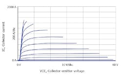
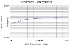
The major task of the test instrument is to provide wide current and voltage measurements. Dependent on the device being tested current requirements can easily be 1000 A or more and voltage can reach 3 kV. Testing the power semiconductor at high currents must be done using a series of short pulses to minimize device heating. Fig. 1 shows a typical a plot of IC vs VCE and Fig. 2 shows the breakdown characteristics of a power MOSFET.
Although no current should flow in the off-state of high power applications, there can often be small leakage currents. This means that even sub-nanoamp current measurements on the power devices may be necessary to guarantee the energy efficiency of the end product. Understanding the maximum current when a device is on and the leakage current when a device is off is important for circuit designers, because these characteristics impact both operating margin and energy efficiency. This means that the tester must have the ability to measure currents as low as picoamps and voltages as low as microvolts in addition to much higher operating currents and voltages.
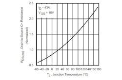
Besides measuring general device characteristics over temperature, the instrument may also be required to screen various devices because they can look fine at room temperature, but be out of spec at a low or high temperature. Unfortunately, temperature characterization of power devices is not easy. Special measurement techniques must be used because these tests require a thermal test chamber whose temperature can take a long time to stabilize, and long cables leading from the chamber to the test equipment can create resistive and inductive oscillation problems. And, some applications may require performing device tests at temperature extremes, such as -50 °C to 250 °C. Fig. 3 is an example of temperature dependence of a power semiconductor that shows the variation of on-resistance vs. temperature.
Depending on device type and the way it is in the circuit, a power semiconductor may be controlled by voltage or current. When evaluating how a device will perform in a circuit it is important for the tester to drive it using the same stimulus it will experience in the actual application. In addition, certain device parameters are best evaluated in a forced current or forced voltage mode. For example, power device on-resistance should be evaluated by forcing a current through the device that matches its specified current. Also, in many cases a power device datasheet does not specify its behavior under actual operating conditions, so a tester will need the ability to characterize the device with the voltage and current levels employed in the actual application.
One type of tester is an SMU (Source Monitor Unit) that can function as either a precision voltage source or a precision current source, and it can also simultaneously and accurately measure both voltage and current. Thus, it would be useful to toggle the internal SMU operation between current source mode and voltage source mode without requiring any physical connection changes. SMUs also have feedback circuitry that monitors the sense terminal and quickly corrects the voltage and current applied to the DUT (device under test) to match its programmed value. SMU technology makes it easy to characterize power devices under the same bias conditions, as they will experience in an actual power electronics circuit.
For all levels of current and voltage, it is important to obtain accurate and reliable measurement results. The larger the measurement error is in device evaluation, the larger the negative impact it has on circuit operating margins and peripheral circuit design. However, test data taken using traditional power device measurement equipment (such as curve tracers) is suspect in terms of measurement accuracy and reliability. Therefore, many circuit designers only use curve tracers to verify gross device functionality, and take the numerical measurement results as only a rough indication of device behavior. Obviously, when the need arises to compare the characteristics of multiple devices or to verify whether a device meets a manufacturer’s specifications, an approximate device characterization data is not meaningful.
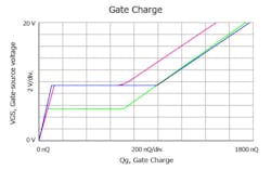
A key parameter to determine from testing is total gate charge (QG), which is the total amount of charge necessary to turn on a power device. It is an extremely important parameter when estimating the driving loss during circuit operation. The driving loss consists of the product of QG, the gate voltage (VG), and the switching frequency. Accurate QG evaluation allows precise driving loss calculation as well as optimized design of the driving circuit. Fig. 4 shows a plot of VGS (gate-source voltage) vs. QG for a super junction MOSFET.
QG also provides other useful information to help with switching operation analysis. For example, when a circuit does not meeting performance expectations, examining the QG curve can offer valuable insights that identify the source of the problem.
Because QG varies with the output voltage and current, it should be evaluated under in-circuit bias conditions. The QG characteristics shown on a device data sheet only provides an approximation of the value of QG during actual circuit operation. Therefore, a test instrument must be able to accurately evaluate QG for both low voltage and high voltage power devices.
Besides driving loss, the instrument should also calculate conduction loss and switching loss. The QG curve can also be interpreted as a representation of the non-linearity of a power device’s stray capacitances. This makes it possible to calculate switching parameters and switching loss using known equations that combine the gate resistance, the resistance in series to the gate, and the switching frequency. The tester should have the ability to accurately measure on-resistance, RDS(ON), and peak current, and also calculate conduction loss. These calculations should be performed automatically by the test instrument for a given frequency.
Understanding the input, output and reverse return capacitances of three terminal devices (such as MOSFETs or IGBTs) is important, because these parameters dictate the switching speed and the switching loss when operating at high frequency. However, accurately measuring these parameters is not easy or straightforward. To make an accurate measurement, the capacitance between two terminals of a three terminal device, the other terminal needs to be appropriately configured (using the capacitance meter’s AC guard output). Depending on the capacitance parameter and type of device being measured, other components (such as an AC blocking resistor or a DC blocking capacitor) may also be needed. In addition, some capacitance measurements need a high voltage bias applied to the DUT, which requires additional components to protect instrument resources from damage in the event of device breakdown. Therefore, a great deal of skill and thought must go into making a single type of capacitance measurement, because it is easy to make a mistake that leads to invalid data collection.
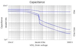
It would be helpful if the tester can automatically and accurately measure FET capacitance values (CISS, COSS, CRSS). This involves using all the resistors, capacitors and protection circuits necessary to make high-voltage capacitance measurements. The tester should automatically arrange these components into the correct configuration for a specified capacitance measurement. Fig. 5 shows a typical presentation of these capacitance values.
An applied DC voltage causes a power device’s depletion region to modulate, which in-turn causes the junction capacitance to vary with voltage. The drain or collector terminal of a power device is often exposed to high voltages when it is off, which determines the value of its junction capacitances at the moment it turns on. Therefore, understanding how device capacitance changes with applied voltage is very important for power electronics circuit designers. Knowing the true value of device capacitance at a specific voltage and the calculated voltage the device will experience in a circuit allows selection of a power device with the lowest loss. To produce reliable capacitance measurements the power device capacitance measurement needs to be performed at relatively high frequencies, so the tester should compensate for the various parasitic elements in the cables and test fixtures.
Gate resistance is an important parameter for circuit designers because it influences device operation speed and switching loss. The tester should be able to measure the device gate resistance (RG) when it performs a capacitance measurement, which eliminates the need for additional complicated data analysis.
Circuit simulators such as SPICE are an essential tool for power electronics circuit designers. Accurately simulating the performance of a circuit can result in significant cost savings through reduced development cycles and prototyping. Therefore, the test instrument should be able to precisely model CRSS, CISS and RG. These device parameters are essential for accurate power circuit simulations.
The tester should be able to measure the key parameters essential for reliable and efficient device performance. Unfortunately, you can never be certain that a power device’s behavior matches the characteristics shown on its device datasheet, and curve tracers can only provide coarse parameters such as breakdown voltage and approximate on-resistance. Modern high-performance power devices exceed the measurement capabilities of traditional curve tracers, which cannot characterize capacitance at all. Understanding the relationship between on-resistance and gate-to-drain capacitance (CGD) is also crucial to optimizing high-speed device performance. To accurately predict device performance, you must measure both on-resistance and capacitance.
A good test instrument can also detect low-cost, low-performance devices and counterfeit devices that often have large junction capacitances even though their measured on-resistance is low. Besides capacitance and on-resistance issues, inferior grade devices also often show severe performance degradation at high temperatures. Detecting counterfeit and inferior power devices offers many obvious cost benefits in terms of reducing design cycles and product liability issues.
When circuits do not perform as expected, a very effective trouble shooting method is to perform a detailed characterization of each power device in the circuit. Many times incorrect circuit operation is due to unforeseen leakage currents or degraded breakdown voltages. Recognizing a bad component can often provide a shortcut to identifying a solution for improper circuit behavior.
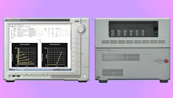
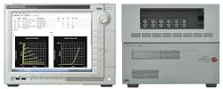
An example of this new generation of power semiconductor test instruments is the Agilent B1506A, shown in Fig. 6. It has three current/voltage versions:
· 20A/3kV
· 500A/3kV
· 1500A/3kV
About the Author

Sam Davis
Sam Davis was the editor-in-chief of Power Electronics Technology magazine and website that is now part of Electronic Design. He has 18 years experience in electronic engineering design and management, six years in public relations and 25 years as a trade press editor. He holds a BSEE from Case-Western Reserve University, and did graduate work at the same school and UCLA. Sam was the editor for PCIM, the predecessor to Power Electronics Technology, from 1984 to 2004. His engineering experience includes circuit and system design for Litton Systems, Bunker-Ramo, Rocketdyne, and Clevite Corporation.. Design tasks included analog circuits, display systems, power supplies, underwater ordnance systems, and test systems. He also served as a program manager for a Litton Systems Navy program.
Sam is the author of Computer Data Displays, a book published by Prentice-Hall in the U.S. and Japan in 1969. He is also a recipient of the Jesse Neal Award for trade press editorial excellence, and has one patent for naval ship construction that simplifies electronic system integration.
You can also check out his Power Electronics blog.
Voice Your Opinion!
To join the conversation, and become an exclusive member of Electronic Design, create an account today!

Leaders relevant to this article:
