Protect A Power Factor Controller Circuit And Battery Charger From Voltage Surges
In a typical ac-dc power supply, diode bridges do not control inrush current due to the output capacitor sudden charge at line plug-in. A high inrush current can cause several issues for the system like component failure (fuse, bridge diode, etc.), but it also represents an excessive current stress for the power grid. If nothing is implemented to limit the inrush current, the start-up current can easily be 10 to 20 times higher than the steady-state current. The power grids components have then to be rated to deliver such a high current for a short time. Moreover, the sudden current variation will lead to line voltage dips. These fluctuations will decrease the power delivered to other loads. Lamps or displays connected on the line could then present a brightness variation called the flicker phenomenon. To avoid such unwanted phenomenon, the IEC 61000-3-3 Electromagnetic standard defines the maximum allowed voltage fluctuation, and therefore the maximum allowable inrush current.
Related Articles
- Back-to-Basics: Power Factor and the Need for Power Factor
- Improved Power-Factor Corrector Further Minimizes Miller Effect
- Online Design Tool Programs Interleaved PFC
- What's The Difference Between Reactive Power Factor And AC-DC Supply Power Factor?
- LED Lighting Management IC Improves Power Factor and Efficiency
- Buck LED driver with Active PFC
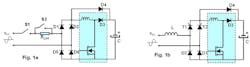
To meet the IEC 61000-3-3 standard the capacitor inrush-current is usually limited by a resistor (RLIM in Fig. 1a, which can be either a fixed-value resistor or a temperature-variable resistor. Temperature-variable resistors usually present a negative thermal coefficient (NTC) so that the resistor will have a high impedance value at cold-state, i.e. at start-up, and a low impedance value at steady-state. The low-value resistor is required at steady-state to limit the power losses dissipated by this resistor. A better solution consists of turning a switch on in parallel to bypass its impedance.
Mechanical relays are usually used for the bypass switch (S2 in Fig. 1a. The drawback of this solution is that the RLIM resistor is always connected to the line and thus supplies the diode bridge even if the application is in stand-by mode. As the DC capacitor (C) is still charged, standby losses will then occur. To suppress these losses, a switch has to be added in series with the line voltage (S1 in Fig. 1a, which is opened to disconnect the diode bridge in stand-by mode.
Another, smarter, solution consists of implementing a mixed bridge as shown in Fig. 1b.
This solution allows the limiting of inrush current by slowly charging the output capacitor with a progressive Silicon Controlled Rectifier (SCR) soft-start. The SCR is triggered at the end of each line half-cycle to apply a reduced voltage to the capacitor. The SCR turn-on delay is then progressively reduced to enlarge the SCR conduction time and increase the energy applied to the DC capacitor.
This solution works if an inductor is present in series with the line (L in Fig. 1b This inductor comes for free as most applications, using a DC bridge, feature an SMPS or a motor inverter that requires a high-frequency switching filter. And most EMI filters feature a common mode inductor that presents a spurious differential-mode inductance.
An auxiliary supply is required in this solution to supply the MCU before the DC output capacitor is charged so that the MCU can ensure the SCR’s soft-start.
The entire solution for an inrush current limiter (ICL) function and stand-by losses suppression is then implemented by two SCRs, instead of one ICL resistor and two mechanical relays. The solid-state technology could then be cheaper than the mechanical technology solution and will suppress following drawbacks of mechanical relays:
· Higher control current consumption due to the coil
· Risk of switch opening in case of machine vibrations
· Acoustic noise due to the mechanical contact
· Risk of explosion in flammable environment (due to switching spark)
· Poor reliability (especially is the relay is switched on or off when a high DC voltage or a high current is present).
Front-End Protection For Voltage Surges
As a mixed bridge, like every diode bridge, is connected directly to the AC line plug, there is a risk of damage to the bridge and the PFC silicon devices (like bypass diode D4 in Fig. 1) if a voltage surge is applied.
According to the IEC61000-4-5 standard that describes how surges must be performed, the surge voltage has to be applied at different angles, and for both positive and negative polarities.
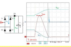
We have performed a 4 kV positive surge test applied at a 90° angle as shown in the simplified schematic of Fig. 2. We used a 2 µH inductor for L and 100 µF for C in order to be close to the worst application case. The SCRs are two TN5050H 1200V 50A thyristor devices, and D1, D2, and D4 diodes (PFC by-pass diodes) are STTH6010WY fast rectifier devices.
For a 90° angle, T1 and D1 are conducting. The surge energy will then increase the current level and will cause D4 to turn-on due to the voltage held by the PFC inductance. Diode D4 thus allows the surge current to be by-passed and avoid damaging the PFC freewheeling diode (D3).
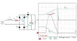
Fig. 2 shows T1 current (so D1 and D4 current too) reaching a 1730 A peak current during the surge. The current pulse width is equivalent to a 30 µs long half-sinus. Such a current stress is well below the STTH6010WY and TN5050H current capability.
In case the applied surge current is above the SCR or diode current capability, there are basically two ways to reduce this overcurrent (both could be used together):
· Increasing the differential inductor will help reduce the applied peak current, but it will also slightly increase the overcurrent pulse width.
· Adding a varistor at Line input will help reduce the peak voltage applied to the circuit, and so the overcurrent as well.
Also shown in Fig. 2. is that the VDC output voltage is increased by the surge current energy to 650 V. This voltage is reversely applied to T2 (as diode D1 is also conducting when T1 is ON) and D2. Devices of at least 800 V have to be used. As the TN5050H and the STTH6010 are respectively a 1200 V and a 1000 V device, the voltage margin is very high.
A better voltage limitation could be brought by using a higher-value output capacitor or a capacitor with a lower internal parasitic series resistor if the reverse voltage exceeds the SCR or diode capability.
Negative Surge Applied At Peak Mains Voltage
If a negative surge is applied with a 90° angle, the mixed bridge behavior is a little bit more complex. Fig. 3 gives the circuit sequences for this case:
· Phase A: normal mixed bridge operation before the surge is applied. VAC voltage is positive, so T1 and D1 are conducting. The line current (IL, cf. dashed green line) is circulating from L to N through T1, D1, and the output capacitor.
· Phase B: a negative voltage surge is applied, and VAC then becomes negative. This means that a negative current (represented by the red dashed Line) will now be circulating from N to L.
· Phase C: the line current has decreased following VAC inversion. When IL current reaches zero, D1 turns off. This means that now the whole line voltage is applied across T2 (cf. VT2 red arrow).
Phase C has to be carefully managed. Indeed, if the voltage increases above the breakdown voltage of the SCR, the device may be damaged by breakover.
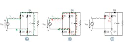
Protection By Transil
To prevent T2 damage during Phase C, one solution is to use a Transil overvoltage protection device connected between the SCR Anode and Gate (Fig. 4.) Transil diodes provide high overvoltage protection by clamping action. Their instantaneous response to transient overvoltages makes them particularly suited to protect voltage sensitive devices, such as MOS technology and low voltage supplies ICs. They are available as either uni-directional or bi-directional types.
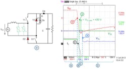
In this case, during phase C, the voltage will increase up to the Transil breakdown voltage (VBR). The Transil diode will then start to conduct and will apply a current to the SCR gate. The SCR will then turn on. Fig. 4 shows such behavior:
· Phase A ends at point 1 where VAC voltage becomes negative.
· Phase B ends at point 2 where line current voltage reaches zero.
· During phase C, T2 turns on at point 3 where the voltage exceeds the Transil breakdown voltage. The maximum voltage applied to T2 is limited to 430 V. Then D2 also turns on and applies the surge energy, which charges the output capacitor.
· Phase D starts after point 4. The surge current is applied to the output capacitor through T2, D2 and D4. T1 and D1 are off.
For the Transil, we used a 1,5KE400CA device for our tests. This diode allows the clamping voltage to be limited to a very low peak level (430 V), and this is a particularly important point. During phase C, the absolute value of the negative voltage applied to D1 equals to the sum of VT2 and VDC. For a 325 V output DC voltage, this means that D1 sees a 755 V negative peak voltage (which is within limits for the STTH6010). A higher voltage transil or a lower energy transil (1,5KE400CA is a 1500 W transil) will lead to a higher clamping voltage and a higher voltage applied to D1.
The resistor connected between T2 gate and the cathode is used to derivate the current coming from Dz Transil diode and avoid spurious triggering by dV/dt
Protection By Varistor
In case a turn-on of the SCR above 430 V is not desired, or in case the surge current exceeds the SCR ITSM capability when the device is triggered by the Transil, there is another solution: using voltage suppressors such as metal oxide varistors at the bridge input (green dashed lines in (Fig. 4) instead of Transil diodes. Varistors are put behind the EMI filter in order to limit their absorbed current thanks to the filter impedance (especially the differential-mode inductance of common-mode choke).
Several varistors can be used in parallel to better clamp the voltage surge and avoid turning on T2 in case of a negative surge applied at a 90° angle (or T1 turn-on in case of a positive surge applied at 270°).
The surge withstanding level will then depend on the varistor capability to clamp the surge voltage below the T1/T2 SCR VDSM/VRSM and D1/D2 diodes VRRM. The SCR overcurrent is no longer an issue. For example, with four 385 V 14 mm Metal Oxide Varistor (MOV) in parallel, and with a typical EMI filter, the mixed-bridge voltage was limited to 1100 V even for a 6 kV surge, which is well below the thyristor TN5050H VDSM capability and typical STTH6010 fast rectifier breakdown voltage. The circuit is then typically able to sustain a 6 kV surge.
About the Author
Comment About the Article
To join the conversation, and become an exclusive member of Electronic Design, create an account today!

Leaders relevant to this article: