Digital Potentiometers Enable Output Voltage Adjustment Of Switched-Mode Supplies
In many system applications, it becomes necessary to adjust a switched-mode power supply (SMPS) output voltage within narrow limits in order to remove tolerances and drops in the power path, verify the operation at the system limits, or to implement simple dynamic voltage control for microprocessors. Also, the system designer may want to adjust supply voltages, either to optimize their levels or to force them away from nominal values when characterizing system performance under extreme conditions. This function is typically performed during in-circuit test (ICT), where a manufacturer wants to guarantee that a product functions correctly at nominal supplies ±10%. This output voltage changing procedure, called margining, deliberately changes the supply voltage within its expected range. Other output changing applications, such as dynamic voltage control for a microprocessor, must be able to change the voltage on fly, reducing the voltage in low power modes and increasing it in high performance modes.
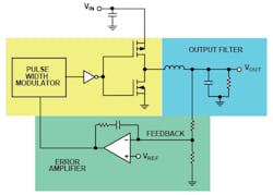
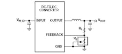
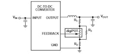
The output voltage of a typical SMPS (Fig. 1) is compared with an internal reference, with the difference connected to the pulse width modulator (PWM).The PWM compares a ramp with the amplifier output, and generates the PWM signal that controls the switches that deliver power to the load.
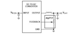
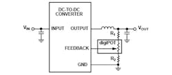
You can adjust the output voltage by controlling the voltage at the error amplifier pin. This can be done externally, using a DAC, or with a digital potentiometer, as shown in Fig. 2. Some voltage regulators allow internal control of the feedback voltage using a serial interface such as PMBus, I2C, or SPI. Table 1 compares three methods in terms of adjustment capability and power dissipation.

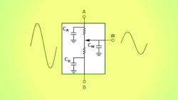
The digital potentiometer, or digiPOT, operates in manner similar to that of a conventional potentiometer with the mechanical wiper action replaced by electronic switches and digital signals, as shown in Fig. 3. The digiPOT employs a string of small resistor in series with an electronic switch located at the intersection of every two resistors. The digiPOT’s resolution depends on number of positions in the resistor network. The higher the number of positions the higher resolution.
Some digital potentiometers are available with non-volatile memory, so the output supply can be programmed in test. This easy-to-use feature provides a substantial benefit, compared to the other two methods.
Linearizing The Transfer Equation
The ratio of feedback resistors R1 and R2 determine the SMPS output voltage.

Where:
VFB = Internal reference voltage
VOUT = Output voltage
R1 = Feedback resistor to Output
R2 = Feedback resistor to Ground
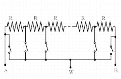
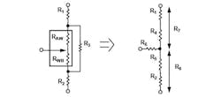
Some issues should be considered before replacing R1 and R2 with a digital potentiometer. Internally, the digital potentiometer has two resistor strings, RAW and RWB, as shown in Fig. 4.

Both string resistors are complementary.
RAW = RAB – RWB (3)
Where:
RAB = End-to-end resistance or nominal value.
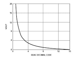
Replacing R1 and R2 with RAW and RWB results in a logarithmic transfer function. The nonlinear relation between the digital code and the output voltage decreases the low-end resolution. Fig. 5 illustrates this logarithmic transfer function from a digital potentiometer.
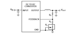
This resolution problem can be overcome in several ways; the more common approach is to use the digital potentiometer in rheostat mode, as shown in Fig. 6, or to place resistors in series with the potentiometer, as shown in Fig. 7.
Minimizing The Tolerance
Due to the resistor tolerance, using a digital potentiometer in conjunction with external resistors can cause mismatch problems. Precision devices might have 1% resistor tolerance, but the vast majority of digital potentiometers can only achieve 20% resistor tolerance.
In this case, reducing the mismatch is possible by using a series/parallel resistance combination, as shown in Fig. 8 and Fig. 9. As a downside, the dynamic range is reduced as well.
In rheostat mode, the series resistance must be high enough to render the tolerance of the digital potentiometer negligible, that is R2 ≥ 10 × RAB. In potentiometer mode, the parallel resistor must be small enough, that is R3 ≤ RAB/10.
Linearizing the potentiometer using a series-parallel combination could be quite complex, as shown in the equivalent circuit of Fig. 10.
Where:


R7 = R1+R4 (6)
R8 = R2+R5 (7)
The feedback input pin typically has high impedance, so the effect of R6 can be made negligible.
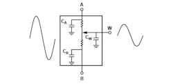
The switching regulator operates at high frequency, typically above 1 MHz, allowing the use of small external components. In worst case scenarios, it must power dynamic loads, so the feedback resistor network must provide enough bandwidth to accurately track the output voltage. Due to the parasitic internal switch capacitance, the digital potentiometer acts as a low-pass filter, as shown in Fig. 11. If the feedback network does not have enough bandwidth, the output voltage may oscillate.
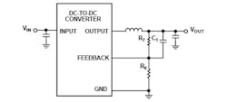
A simple way to overcome this limitation is to place a capacitor in parallel between the output and the feedback network, as shown in Fig. 12, reducing the high frequency impedance, and minimizing the oscillation time.
Simpler Solution
Analog Devices’ AD5141 digiPOT overcomes some problems presented by other digital potentiometers. It provides:
• Non-volatile 256-position adjustment
• 10 kΩ and 100 kΩ resistance options
• 8% maximum resistor tolerance
• ±6 mA wiper current
• 35 ppm/°C temperature coefficient:
• 3 MHz bandwidth:
• < 75 μS start-up time
• Linear gain setting mode
• Single- and dual-supply operation
• 1.8 V to 5.5 V independent logic supply
• −40°C to +125°C operating temperature
• 3 mm × 3 mm LFCSP package
• 4 kV ESD protection
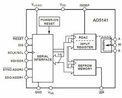
The AD5141 (Fig. 13) operates as true variable resistors for analog signals within the terminal voltage range of VSS < VTERM < VDD. The resistor wiper position is determined by the RDAC register contents. The RDAC register acts as a scratchpad register that allows unlimited changes of resistance settings. A secondary register (the input register) can be used to preload the RDAC register data.
The low resistor tolerance and low nominal temperature coefficient simplify open-loop applications as well as applications requiring tolerance matching.
The main benefit of the AD5141 is the new patented feature implemented called linear gain setting mode. This mode allows independent programming of the resistance between the digital potentiometer terminals, through RAW and RWB string resistors, so:
RAW ≠ RAB - RWB) (8)
Enabling this mode, no external resistors are needed to achieve linear SMPS voltage adjustment , the resistor tolerance becomes negligible, and the overall error of the transfer function is due only to the internal string mismatch, which is typically less than 1% as well as low temperature drifts.
Each string resistor has an associated EEPROM location, so an independent value for each string can be loaded upon power-up. In addition, the device provides up to 3 MHz bandwidth for a fast feedback loop.
The high bandwidth and low total harmonic distortion (THD) ensure optimal performance for ac signals, making it suitable for filter design. The low wiper resistance of only 40 Ω at the ends of the resistor array allows pin-to-pin connection.
Wiper values can be set through an SPI-/I2C-compatible digital interface that is also used to read back the wiper register and EEPROM contents.
The RDAC register can be programmed with any position setting using the I2C or SPI interface, which are hardware-selectable using the DIS pin. When a desirable wiper position is found, this value can be stored in the EEPROM memory. Thereafter, the wiper position is always restored to that position for subsequent power-ups. The storing of EEPROM data takes approximately 18 ms; during this time, the device is locked and does not acknowledge any new command, preventing any changes from taking place. The fast start-up time <75 µS guarantee a quick register refreshment after a power supply sequence.
About the Author
Comment About the Article
To join the conversation, and become an exclusive member of Electronic Design, create an account today!

Leaders relevant to this article: