Integrated Power Stage Modules Support High Current Processors
In 2004, Intel specified a standard integrated Driver-MOSFET (DrMOS) device for use in a typical PC platform. This specification’s goal was to provide features for an integrated device to produce the necessary high current power source for processors. Recently, Texas Instruments introduced a device that has similar functionality, but a different package and design features that take advantage of technology that is 10 years newer than the original Intel specification.
Related Articles
- Designing with DrMOS, Part 1: Concept and Features
- Designing with DrMOS, Part II: Application Guidelines
- Chip-Embedded Packaging Contributes to New Performance Benchmark for DrMOS
- Power Management 101 Series: Power Management Semiconductors
- New Breed of MCMs Optimize System Performance and Cost
- Building Block Modules Power Supercomputers
First, we need to explain the reason for the DrMOS specification. It was based on the power requirements for microprocessors that increase with every process generation. This specification reflected the need for increased static (steady state) and dynamic (transient) power that the processor Voltage Regulator (VR) requires at very low voltages (~1 V) and very high currents (100+A). Intel said this trend will continue in the future with power requirements driven by two technology factors:
· A need for increased power density in the VR to satisfy higher power transfer in a limited real estate environment (such as a desktop computer).
· A need for increased efficiency at higher switching frequencies (a result of a need for faster dynamic response) to maintain losses at low levels.
These two requirements have advanced the designs of VR building blocks employing power MOSFETs. These power semiconductor switches have been used in synchronous buck converters, which have remained the main workhorse for the voltage regulators feeding microprocessors. Due to the nature of the voltage conversion ratio needed in the VRs, these power switches have been optimized for characteristics that reduce losses. In the DrMOS the concept has been moved further by integrating the power switches and their drivers into a single module that provides improved performance and cuts pc board real estate requirements.
In addition, technology has advanced since the original DrMOS of 2004:
· Power MOSFET technology has improved in the past 10 years, with lower RDS(ON) and improved Figure of Merit (RDS(ON) ×QG).
· Vertical power MOSFETs now offer better high power characteristics than lateral structures.
· Integrating driver and power MOSFETs physically close to each other in a single package improves switching speed, reduces the device’s PCB footprint, and allows reduced dead time in a multiphase circuit.
· New techniques shrink package size and reduce loop inductance, improving switching speed.
Several semiconductor companies followed the Intel specification with single chip power modules. Among DrMOS suppliers are Alpha and Omega Semiconductor, Fairchild Semiconductor, Infineon, International Rectifier, Intersil, ON Semiconductor, Toshiba, Vishay Siliconix, and ZMDI.
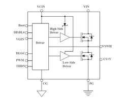
Fig. 1 is a diagram of the basic DrMOS circuit. It consists of a high side (HS) and low side (LS) power MOSFET along with their associated drivers. This is the basic circuit, but companies may add enhancements as long as they meet all other requirements of the Intel specification.
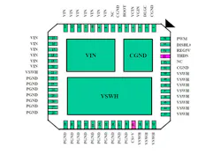
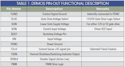
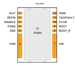
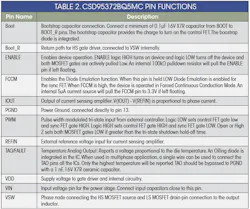
Table 1 lists the pin functions of a DrMOS module and Fig. 2 shows the layout of the Intel specified DrMOS that is in an 8mm x 8 mm, 56-pin PQFN package.
Texas Instruments’ CSD95372BQ5M/C NexFET™ smart power stage is a high performance low voltage MOSFET pair combined with a driver IC that is functionally similar to Fig. 1, with some added enhancements. This highly optimized design is intended for a high-power, high-density synchronous buck converter used in either single or multi-phase POL applications. The device integrates an optimized driver IC and NexFET silicon that achieves high efficiency using a PowerStackTM configuration. This combination produces high current, high efficiency, and high speed switching capability in a high density, 12-pin, SON 5 mm x 6 mm package.
It also integrates the accurate current sensing and temperature sensing functionality to simplify system design and improve accuracy. In addition, the PCB grounded lead footprint has been optimized to improve thermal performance and simplify the completion of the overall system design. The CSD95372BQ5M/C features integrated current feedback with three per cent accuracy that eliminates the need for inductor DC resistance (DCR) sensing.
TI’s CSD95372BQ5M/C offers an optional DualCool™ NexFET™ power MOSFET package enabling thermally efficient cooling through the top and bottom of the package. This package allows power system designers to effectively direct heat away from the PCB in high-current DC/DC applications, resulting in improved power density, higher current capability and improved system reliability.
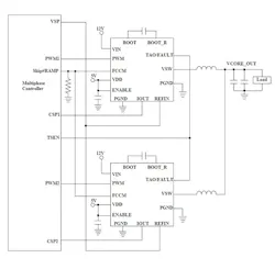
A typical application for the CSD95372BQ5M/C employs a multiphase controller driving a two-phase buck converter (Fig. 3).
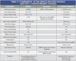
Table 3 compares the features for a VR implementation with DrMOS and the TI CSD95372BQ5MC. DrMOS features are not meant to restrict the development of other design features that could improve module performance. The parameters in the table should be taken as a guideline given the requirements of voltage regulators in a desktop environment. Also, the detailed electrical characteristics pertaining to switching times, logic level requirements are not given so that each module developer can innovate within a given set of features.
About the Author

Sam Davis
Sam Davis was the editor-in-chief of Power Electronics Technology magazine and website that is now part of Electronic Design. He has 18 years experience in electronic engineering design and management, six years in public relations and 25 years as a trade press editor. He holds a BSEE from Case-Western Reserve University, and did graduate work at the same school and UCLA. Sam was the editor for PCIM, the predecessor to Power Electronics Technology, from 1984 to 2004. His engineering experience includes circuit and system design for Litton Systems, Bunker-Ramo, Rocketdyne, and Clevite Corporation.. Design tasks included analog circuits, display systems, power supplies, underwater ordnance systems, and test systems. He also served as a program manager for a Litton Systems Navy program.
Sam is the author of Computer Data Displays, a book published by Prentice-Hall in the U.S. and Japan in 1969. He is also a recipient of the Jesse Neal Award for trade press editorial excellence, and has one patent for naval ship construction that simplifies electronic system integration.
You can also check out his Power Electronics blog.
Voice Your Opinion!
To join the conversation, and become an exclusive member of Electronic Design, create an account today!

Leaders relevant to this article:
