Inverted and Automated: Acoustic Sorting of IGBT Modules
The long-term reliability of power IGBT modules depends strongly on the structural integrity of the module. Since their introduction in the 1980s, IGBT modules have accelerated the transition from single-speed motor driving to variable speed motor driving. The applications are numerous and significant: industrial equipment, railroads, household appliances such as air conditioners, and electric vehicles. The key benefit of variable motor speed is significant energy savings.
Related Articles
- Acoustic Imaging Of IGBT Modules Through The Heat Sink
- Title
- Inverted Acoustic System Cuts IGBT Failures
- Acoustically Mapping IGBT Module Solder Thickness
- Power Device Evaluation At Temperature With Integrated Hot Plate
- Comprehensive Power Semiconductor Testing Ensures Optimal Device Selection
Structural integrity of the module means the absence of voids, delaminations, non-bonds, cracks and other conditions that can cause the module to fail. A chief cause of failure is overheating and electrical failure of the die. Because the die put out high levels of heat that must be dissipated before damage can occur, voids and other gap-type internal features that impede or block the dissipation of heat through the metal heat sink at the bottom of the module can cause electrical failure.
In the past few years, acoustic micro imaging tools that can reliably and nondestructively recognize, image and analyze these unwanted internal features have been developed by Sonoscan. This article describes the latest and, in terms of production of IGBT modules, the most significant tool: a fully automated acoustic microscope system that automatically loads, images, and unloads the modules, and reports the status of each module. The microscope scans multiple modules at a time, and needs no human operator after initial startup.
This tool serves as a dedicated, non-stop sorting machine that intelligently and quickly separates accepts from rejects, and is commonly used before encapsulation of the module. Rejects are not merely identified as rejects; the acoustic data and images reveal the type of rework that can turn them into accepts on the next inspection. Occasionally modules are inspected after encapsulation as a final test protocol before shipping. The tool is also used to inspect field failures before Destructive Physical Analysis (DPA) is performed.
At the beginning of an inspection run, IGBT modules are stacked with the die side up and with the heat sink down at one end of the system. A technician uses the system keyboard to select the recipe for scanning the specific module type. He clicks a box to begin the inspection sequence. From this point on operation is automated and the technician is not needed.
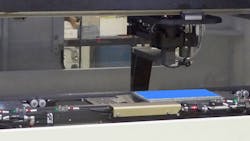
A conveyor places places a module from the stack onto each of the tool’s two (or more) stages. The module fits precisely into a cutout in the stage; each module type has its own cutout, which supports the periphery of the module and which acts as a water barrier (Fig. 1). The modules in Fig. 1 are masked in blue to preserve proprietary features.
The transducer, and its water jet, are positioned below the stage. Conventionally, items being imaged by an acoustic microscope are imaged from their top sides. Power IGBTs cannot be fixtured in this way, because even brief exposure to water may deposit, on evaporation, a residue that could become a leakage path. This is why Sonoscan has inverted both the transducer and the water column that couples the transducer to the surface of the heat sink. The design of the template into which the IGBT module fits so precisely prevents water from the water column from reaching the top of the stage. Other barriers in the stage make it essentially waterproof. The water column is needed because ultrasound at the high frequencies used in acoustic microscopes travels poorly or not at all though air.
When the transducer begins raster-scanning the bottom surface of the module, it performs its pulse-echo function thousands of times per second. The forward speed of the transducer reaches more than 1 m/s. More important, its average speed throughout the scan process is the highest in the industry. The speed of ultrasound through the materials in the module is very high. Through silicon, for example, its velocity is 8433 m/s; through copper, 4660 m/s. The result is that the transducer can pulse and receive echoes from thousands of pulses, representing thousands of x-y coordinates, per second.
Automated tools already in the field are being used extensively to image the solder layer that bonds the heat sink to the ceramic raft above it. To do so, the return echoes are gated on a depth extending from the top of the solder layer to the top of the raft. Pixels are collected only from echoes within this depth; echoes from other depths, all the way up to the die, are ignored when inspecting for voids and other anomalies in the solder layer.
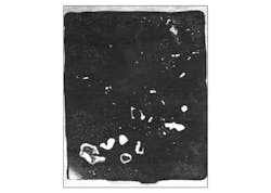
Fig. 2 is the monochrome acoustic image of the solder layer between the heat sink and one raft of a fairly large IGBT module. The irregularly shaped white features, large and small, are voids, delaminations or other gap-type defects in the solder. When a pulse of ultrasound encounters such a defect, it strikes the solid-to-air interface, which reflects >99.99% of the ultrasound. This very high amplitude means that such interfaces are imaged in white in monochrome images. The remaining areas of the solder reflect no ultrasound, although the solid-to-solid interface where the solder meets the raft will reflect a modest percentage and thus, as here, appears dark gray.
Users of the tool are interested in the location and area of each gap-type anomaly, since these anomalies block heat that must be dissipated to avoid electrical failure. The total area of the anomalies below a given raft is an important measurement. So are the locations of the anomalies. In a module of a given design, a void that is directly below a die may be more risky that one that is not directly below a die. The user, who has information about structure and the failure history of a given IGBT module, can thus define his accept/reject criteria very precisely.
When scanning of a module has been completed, analysis of the data has already been accomplished. A conveyor moves each module to one of two stacks at the other end of the system. One stack is for rejects, the other for accepts. The data on each module is typically stored in the user’s Factory Information System; it may also be stored locally. But the paramount job of sorting has been completed, and the accepts can move forward in the line. A technician may view images of the rejects individually to judge each one’s suitability for rework.
The description above applies to purely production inspection, where the emphasis is on inspecting a single depth of great interest. It uses C-mode imaging, where echoes reflected from material interfaces are given a pixel value according to the amplitude of the echo. During transducer scanning, each of the x-y coordinates returns not one but many echoes. In C-mode imaging, the echo having the highest amplitude at each x-y coordinate is used to assign the brightness value to the pixel. An echo from the solid-to-air interface at the top of a void, for example, would produce a bright white pixel because virtually all of the ultrasound is reflected. The solid-to-solid interface between the solder and the ceramic raft will be some shade of gray, the echo amplitude (and thus the shade of gray) being determined by the physical differences between the two materials at the interface.
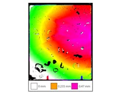
There are other imaging modes that can be used to improve sorting by changing the way in which the echoes are used. One is demonstrated in Fig. 3, which is the same raft area as in Fig. 2. The colors seen here do not identify defects. Instead, they indicate the depth of a specific feature - in this case, the interface between the raft and the solder layer. The Profile Mode™ was used, which measured the time of flight of the echo from the interface of interest to the top surface of the solder at each x-y coordinate that the transducers scans.
To make this image, a gate was set from just below the top of the solder layer to just beyond the lowest point on the raft. The heat-sink-to-solder interface was omitted to avoid having two interfaces covering the whole area of the image. The distances given in Fig. 3 are the approximate thickness of the solder for each of the three colors.
In this image, the raft is clearly warped. In the bright green region at the right, the time of flight (distance) is greatest. Moving to the left - cyan, teal, etc.- the time of flight drops, indicating that the interface moves closer to the transducer, and that the solder becomes thinner. In the bottom left corner, the small black region indicates that the solder layer is either absent or not bonded. The significant changes in distance across the raft reveal that the raft is warped, and that its warp has made the solder thickness uneven.
The irregularly shaped features are gap-type defects such as voids and delaminations. Many of these features are black because they are above the gated depth: ultrasound reflected from the raft-solder interface is locally blocked by these features, which are therefore imaged as dark acoustic shadows. But some of the smaller gap-type defects are within the gated depth, and have the color (magenta, for example) that corresponds to their depth.
About the Author
Voice Your Opinion!
To join the conversation, and become an exclusive member of Electronic Design, create an account today!

Leaders relevant to this article:


