Back to Basics: Voltage Regulator ICs, Part 1
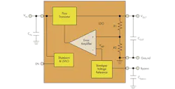
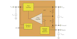
Among regulators, the simplest regulator circuit is for a low-dropout (LDO) voltage regulator whose topology is shown in Fig. 1. As a linear voltage regulator, its main components are a pass transistor, error amplifier, voltage reference, and output power MOSFET. One input to the error amplifier, set by resistors R1 and R2, monitors a percentage of the output voltage. The other input is a stable voltage reference (VREF). If the output voltage increases relative to VREF, the error amplifier changes the pass-transistor’s output to maintain a constant output voltage (VOUT).
Fig. 1. An LDO’s low dropout voltage and low quiescent current make it a good fit for portable and wireless applications.
Low dropout refers to the difference between the input and output voltages that allows the IC to regulate the output voltage. That is, the LDO regulates the output voltage until its input and output approach each other at the dropout voltage. Ideally, the dropout voltage should be as low as possible to minimize power dissipation and maximize efficiency.
The major advantage of an LDO IC is its relatively “quiet” operation because it does not involve switching. In contrast, a switch-mode regulator typically operates between 50 kHz and 1 MHz, which can produce EMI that affects analog or RF circuits. LDOs with an internal power MOSFET or bipolar transistor can provide outputs in the 50 to 500 mA range. The LDO’s low dropout voltage and low quiescent current make it a good fit for portable and wireless applications.
Related Articles
- Power Management Basics: Power Management System Considerations
- Power Management 101: Converter & Controller ICs
- Power Management Basics: Power Supply Fundamentals
An LDO regulator’s dropout voltage determines the lowest usable input supply voltage. That is, although specs may show a broad input voltage range, the input voltage must be greater than the dropout voltage plus the output voltage. For a 200 mV dropout LDO, the input voltage must be above 3.5 V to produce a 3.3 V output.
With an LDO, the difference between input voltage and output voltage may be small, and the output voltage must be tightly regulated. Plus, transient response must be fast enough to handle loads that can go from zero to tens of amperes in nanoseconds. Further, output voltage can vary due to changes in input voltage, output load current, and temperature. Primarily, these output variations are caused by the effects of temperature on LDO voltage reference, error amplifier, and its sampling resistors (R1 and R2).
SWITCH-MODE REGULATORS
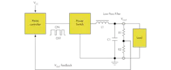
In many applications linear supplies have been superseded by switch-mode supplies. Shown in Fig. 2 is a typical isolated switch-mode supply.
Fig. 2. Switch-mode power supply turns the input dc on and off, then rectifies it to obtain a dc output.
One widely used approach uses the on and off times of pulse-width modulation (PWM) to control the power switch output voltage. The ratio of on time to the switching period time is the duty cycle. The higher the duty cycle, the higher the power output from the power MOSFET switch. A low-pass filter connected to the output transformer provides a voltage proportional to the ON and OFF times of the PWM controller. In operation, a fraction of the dc output voltage feeds back to the error amplifier, which causes the comparator to control the PWM ON and OFF times. If the output voltage changes, the feedback adjusts the duty cycle to maintain the output voltage at the desired level.
To generate the PWM signal, the error amplifier accepts the feedback signal input and a stable voltage reference to produce a output related to the difference of the two inputs. The comparator compares the error amplifier’s output voltage with the ramp (sawtooth) from the oscillator, producing a modulated pulse width. The comparator output is applied to the driver, whose output goes to the power MOSFET.
The inductor-capacitor low pass output filter converts the switched voltage from the switching transformer to a dc voltage. The filter is not perfect so there is always some residual output noise called ripple. The amount of ripple depends on the effectiveness of the low pass filter at the switching frequency. Power supply switching frequencies can range between 100kHz to over 1MHz. Higher switching frequencies allow the use of lower value inductors and capacitors in the output low pass filter. However, higher frequencies can also increase power semiconductor losses, which reduce power supply efficiency.
In terms of power dissipation, the power switch is key component in the switch-mode power supply. The switch is usually a power MOSFET that operates in only two states - on and off. In the off state the power switch draws very little current and dissipates very little power. In the on state the power switch draws the maximum amount of current, but its on-resistance is low, so in most cases its power dissipation is minimal. In the transition from the on state to the off state and off to on the power switch goes through its linear region where it consumes some power. The total losses for the power switch is therefore the sum of the on and off state losses plus the losses in the transition through its linear region.
CONVERTER ICs
ICs for switch-mode power supplies are found either of two basic configurations: converter and controller ICs.
Converter ICs provide a complete dc-dc converter in a single package. The only required external components are usually passive devices. Power switches may be either a bipolar or MOSFET device capable of handling the required current and power. Typically, the power semiconductor switch turns on and off at a frequency that may range from 100 kHz to 1 MHz, depending on the IC type. Most power switches employ pulse width modulation to control the output voltage, so the duty cycle varies according to the desired output voltage.
A controller IC requires an external power switch, either a bipolar transistor or power MOSFET. The controller circuit that employs an external power switch usually has higher efficiency than the converter with an integrated power MOSFET because integrated MOSFETs have a higher on-resistance (higher losses). On-resistance of an external power MOSFET is lower and the MOST usually has higher power output capability than an IC with an integrated MOSFET.
For both converter and controller ICs, the switching frequency determines the physical size and value of filter inductors, capacitors, and transformers. The higher the switching frequency, the smaller the physical size and component values. To optimize efficiency, magnetic core material for the inductor and transformer should be consistent with the switching frequency. That is, the transformer/inductor core material should be chosen to operate efficiently at the switching frequency.
DC-DC converters accept a dc input and produce a dc output. They can be isolated or non-isolated, which depends on whether there is a direct dc path from the input to the output. An isolated converter (Fig. 2) employs a transformer to provide isolation between the input and output voltage. The non-isolated converter employs an inductor-capacitor filter and an optocoupler usually provides isolation between the output feedback and the input. For many applications, non-isolated converters are appropriate. An advantage of the transformer-based converter is that it has the ability to easily produce multiple output voltages using multiple secondary windings.
Initially, integrated power switch converters used bipolar power switches, but virtually all newer devices employ MOSFET power switches that improve efficiency. Another efficiency improvement is the use of integrated synchronous rectifiers consisting of power MOSFETs switches that rectify the power supply output and provide a dc output.
Among the features found in converter and controller ICs:
•Fixed or an adjustable output voltage
•Single-ended or synchronous outputs
•Soft-start that causes the output to come up gradually
•Undervoltage lockout
•Thermal shutdown
•Overcurrent protection
•Overvoltage protection
CHARGE PUMP ICS
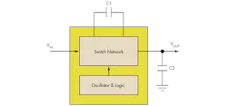
Charge pumps are actually a different form of switching supply. They switch capacitors to provide dc-dc voltage conversion using a switch network to charge and discharge one or more capacitors. The switch network toggles between charge and discharge states of the capacitors. As shown in Fig. 3, the “flying capacitor “ (C1) shuttles charge, and the “reservoir capacitor “ (C2) holds charge and filters the output voltage.
Fig. 3. An advantage of the charge pump is elimination of the magnetic fields and EMI that comes with an inductor or transformer.
The basic charge pump lacks regulation, which is generally added using either linear regulation or charge-pump modulation. Linear regulation offers the lowest output noise, and therefore provides better performance. Charge-pump modulation offers more output current for a given die size (or cost), because the regulator IC need not include a series pass transistor.
A major advantage of the charge pump is elimination of the magnetic fields and EMI that comes with an inductor or transformer. There is one possible EMI source - the high charging current that flows to a “flying capacitor” when it connects to an input source or another capacitor with a different voltage.
MOSFET because integrated MOSFETs have a higher on-resistance (higher losses). On-resistance of an external power MOSFET is lower and the MOST usually has higher power output capability than an IC with an integrated MOSFET.
For both converter and controller ICs, the switching frequency determines the physical size and value of filter inductors, capacitors, and transformers. The higher the switching frequency, the smaller the physical size and component values. To optimize efficiency, magnetic core material for the inductor and transformer should be consistent with the switching frequency. That is, the transformer/inductor core material should be chosen to operate efficiently at the switching frequency.
DC-DC converters accept a dc input and produce a dc output. They can be isolated or non-isolated, which depends on whether there is a direct dc path from the input to the output. An isolated converter (Fig. 2) employs a transformer to provide isolation between the input and output voltage. The non-isolated converter employs an inductor-capacitor filter and an optocoupler usually provides isolation between the output feedback and the input. For many applications, non-isolated converters are appropriate. An advantage of the transformer-based converter is that it has the ability to easily produce multiple output voltages using multiple secondary windings.
MULTIPLE OUTPUT CONVERTER/REGULATOR ICS
Multiple output controller ICs consist of two or more regulators in a single package. They could be two switch-mode converters or two LDO regulators.
An example of a dual switch-mode regulator is a dual current mode PWM step-down dc-dc converter with internal 2 A power switches, this IC operates from a 3.6 V to 25 V input, enabling it to regulate a wide variety of power sources such as four-cell batteries, 5 V logic rails, unregulated wall transformers, lead acid batteries and distributed-power supplies. The two regulators share common circuitry including input source, voltage reference and oscillator, but are otherwise independent. Their feedback loop controls the peak current in the switch during each cycle. This current mode control improves loop dynamics and provides cycle-by-cycle current limit.
An example of a dual-output, low-dropout voltage regulator IC has integrated reset, power on reset (POR) and power good (PG) functions. Differentiated features, such as accuracy, fast transient response, supervisory circuit (power on reset), manual reset input, and independent enable functions provide a complete system solution. These voltage regulators have extremely low noise output performance without using any added filter bypass capacitors and are designed to have a fast transient response and usually stable with low ESR capacitors.
This LDO family also can feature a sleep mode; applying a high signal to either enable input shuts down Regulator 1 or Regulator 2, respectively. Putting the regulators in the sleep mode reduces the input current at TJ = 25°C. Each regulator, has an internal discharge transistor to discharge the output capacitor when the regulator is turned off (disabled).
Multiple output controller ICs can also consist of two or more charge pump converters in a single package. They can be controllers that employ external power switches or regulators with an internal power switch. One possibility is a 5 V output and a 3.3 V output for processor and logic applications.
For example, a typical multiple output charge pump controller ICs can step-down dc-dc converters that produce two adjustable regulated outputs from a single 2.7 V to 5.5 V input. The IC uses switched capacitor fractional conversion to achieve a typical efficiency increase of 50% over that of a linear regulator. No inductors are required.
The IC has two switched capacitor charge pumps to step down VIN to two regulated output voltages. The two charge pumps operate 180° out of phase to reduce input ripple. Regulation is achieved by sensing each output voltage through an external resistor divider and modulating the charge pump output current based on the error signal. A two-phase, non-overlapping clock activates the two charge pumps running them out of phase from each other.
SYNCHRONOUS RECTIFICATION
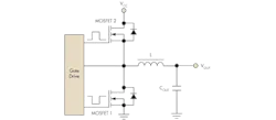
Efficiency is an important criterion in designing dc-dc converters, which requires low power. These losses are caused by the power switch, magnetic elements, and the output rectifier. Reduction in power switch and magnetics losses require components that can operate efficiently at high switching frequencies. Output rectifiers can be Schottky diodes, but synchronous rectification (Fig. 4) consisting of power MOSFETS provide higher efficiency.
Fig. 4.The synchronous rectifier is more efficient than a Schottky diode rectifier.
MOSFETs exhibit lower forward conduction losses than Schottky diodes. Unlike conventional diodes that are self-commutating, the MOSFETs turn on and off by means of a gate control signal synchronized with converter operation. The major disadvantage of synchronous rectification is the additional complexity and cost associated with the MOSFET devices and associated control electronics. At low output voltages, however, the resulting increase in efficiency more than offsets the cost disadvantage in most applications.
UPCOMING TOPICS
There are other key regulator topologies. Next month, we will discuss the two basic IC topologies employed in dc power sources: the step-down, or buck converter and the step-up, or boost converter. Buck topology is a non-isolated power management configuration whose advantages are simplicity and low cost. The boost converter employs a switching technique that causes current to build up in an inductor and then stores the resulting voltage in an output capacitor. Multiple switching cycles build the output capacitor voltage so that the output voltage is higher than the input.
About the Author

Sam Davis
Sam Davis was the editor-in-chief of Power Electronics Technology magazine and website that is now part of Electronic Design. He has 18 years experience in electronic engineering design and management, six years in public relations and 25 years as a trade press editor. He holds a BSEE from Case-Western Reserve University, and did graduate work at the same school and UCLA. Sam was the editor for PCIM, the predecessor to Power Electronics Technology, from 1984 to 2004. His engineering experience includes circuit and system design for Litton Systems, Bunker-Ramo, Rocketdyne, and Clevite Corporation.. Design tasks included analog circuits, display systems, power supplies, underwater ordnance systems, and test systems. He also served as a program manager for a Litton Systems Navy program.
Sam is the author of Computer Data Displays, a book published by Prentice-Hall in the U.S. and Japan in 1969. He is also a recipient of the Jesse Neal Award for trade press editorial excellence, and has one patent for naval ship construction that simplifies electronic system integration.
You can also check out his Power Electronics blog.
Voice Your Opinion!
To join the conversation, and become an exclusive member of Electronic Design, create an account today!

Leaders relevant to this article:
