Power MOSFETs Suppress Noise in Motor-Control Circuits
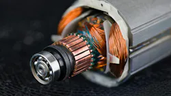
Vishay Intertechnology introduced a new series of 40-V n-channel power MOSFETs optimized for the noisy environments of motor-control circuits.
The new devices — the SIR5402DP, SIR5404DP, SIR5406DP, and SIR5408DP — are all specifically designed to reduce the risk of unintended switching induced by the gate while limiting switching losses caused by gate noise. Vishay said it addressed the first problem by increasing the minimum gate-source threshold voltage to more than 2.5 V and confronted the second by reducing the QGD/QGS ratios to less than 1.0.
The higher gate-source threshold voltage helps prevent unintended turn-on of the MOSFET in motor-drive circuits, where fast switching speeds can lead to high dv/dt rates. That, in turn, can cause significant LC oscillations between the parasitic inductance of the PCB traces and parasitic capacitance in the MOSFET package. This switching noise may increase the gate voltage enough that it turns on the power transistor, impacting the system’s performance and potentially damaging the power stage in the motor driver.
At the same time, the improved gate-charge ratio further reduces gate-induced voltage fluctuations and the impact of gate noise, improving switching stability and reliability along with overall circuit robustness, said Vishay.
These noise-rejection characteristics are suitable for synchronous rectification and DC-DC conversion stages in brushless DC (BLDC) motor drives, cordless power tools, drones, and other systems requiring reliable operation in noisy conditions. By mitigating the effects of gate noise, the devices also deliver higher performance by reducing the risk of unwanted switching and the power losses that come with it.
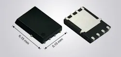
Housed in a compact PowerPAK SO-8 package measuring 6.15 × 5.15 mm, they undergo rigorous testing to verify device robustness.
The devices strike a balance between conduction losses and switching performance with typical on-resistance (RDS(on)) values ranging from 0.9 m to 2.5 mΩ at a gate drive of 10 V and gate charge (QG) values from 32.6 to 82 nC.
About the Author
 James Morra
James Morra
Senior Editor
James Morra is the senior editor for Electronic Design, covering the semiconductor industry and new technology trends, with a focus on power electronics and power management. He also reports on the business behind electrical engineering, including the electronics supply chain. He joined Electronic Design in 2015 and is based in Chicago, Illinois.