Proper Layout Solves Most Power MOSFET Design Problems
"With great power comes great responsibility," says Spider-Man's wise Uncle Ben. Who knew he was really talking about electronic design, FETs, source nets, and switching frequencies?
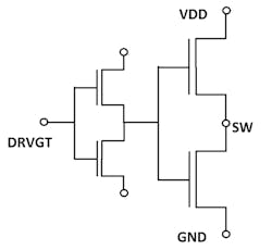
Power MOSFETs are both simple and complex. Compared to designing DRAM or microprocessors, MOSFETs might seem pretty straightforward (Fig. 1). But engineers who create them know that’s not the case. One challenge comes from managing the inrush current versus time. Too fast and you burn out the device. Too slow and you're wasting time, performance, and efficiency. MOSFET designers are responsible for getting the balance exactly right. Meeting this challenge becomes a lot easier when engineers have the right tools.
Most of the problems with high-density and high-speed MOSFETs can be traced to their physical layout, which isn’t intuitive. Designers usually focus on the metric of RDS(on), the resistance between the source and drain when the device is on. This simple model is misleading. Although this model has been accepted for years, modern power designs demand accuracy and applicability that erode with faster switching speeds, high power density, and the quest for higher efficiency. Engineers require a precise modeling tool.
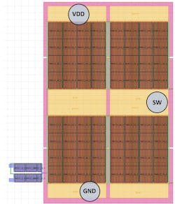
Figure 2 shows the physical layout of a MOSFET output stage arranged as four quadrants of 16 devices each, for a total of 64 instances. Drivers are in the lower-left corner (in blue), with bonding pad locations at top, bottom, and center.
At first glance, this seems like a perfectly reasonable, real-world layout. However, lurking in this design are potential reliability problems, nonuniform switching issues, lost efficiency, overly large dead times, EM violations, voltage-drop issues, thermal issues, and damaging shoot-through current.
None of these problems are obvious from the floorplan. Neither are the circuit-design and schematic issues. MOSFET design is entirely layout-dependent and can’t be uncovered by conventional static lumped models. A detailed, dynamic, and distributed analysis will reveal its hidden flaws.
A Good Start
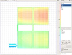
Tackling these design challenges starts at the metallization layers (Fig. 3). The plot shows the potential distribution in the gate net of the output stage at a given time during switching. The colors represent voltage potentials (differences) across the die, with the lowest potential (in blue) naturally nearest near the drivers. The upper right corner diagonally opposite the drivers is substantially underpowered, with over 2 V of difference—even with two metal layers that cover the entire device and a conductor on the left connecting the upper and lower halves.
Due to the inescapable capacitance, resistance, and inductance found in most devices, it will take a finite amount of time to charge and discharge these nets. This is particularly true at higher switching speeds, where once-simple designs start to behave like clocking circuits. For this reason, MOSFETs are designed with a built-in time delay between high-side and low-side switching. The high side must be off entirely before the low side comes on; otherwise, there will be current shoot-through.
Designers often take a conservative approach and delay high-side switching, packing on a safety margin so that the device won't fail under operating conditions. Unfortunately, this technique leaves performance on the table, unnecessarily increasing dead time and reducing switching speed.
It makes more sense to measure, predict, and model the device's actual behavior during layout. Performance can be dialed up to its maximum extent without compromising reliability, requiring expensive experimentation, or needing to make frequent layout changes.
Power-device metrics like RDS(on) are complex and include channel, accumulation layer, drift region, metallization, bond wires, and package parasitics. They also change with temperature and with current. It's impossible to model the circuit behavior using a simple lumped model, whereas a distributed model produces accurate results.
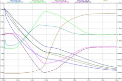
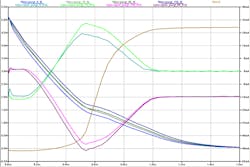
Figure 4 plots voltage (left axis) and current (right axis) from the four quadrants of the die, as well as the global switching output (in brown). All four voltage measurements start at 5.0 V and decline to near zero over the span of about 1.6 ns, as expected. Ideally, all four plots would lie atop one another, indicating simultaneous switching behavior. Instead, there's as much as 1.0-V difference between supposedly identical instances.
Similarly, the four current traces show differing currents in different areas of the device.
The Fix Is In
The solution lies not in changing the MOSFET circuity itself, but in tweaking the layout, specifically the gate routing. By making two small alterations, we can improve the behavior of the device.
Figure 5 shows the revised layout with a second north-south bus in the center of the die, as well as an almost unnoticeable change to the existing bus on the left side. Rerunning the dynamic model shows improved switching behavior, compared to the initial results from Figure 3.
More importantly, the device's dynamic behavior is also improved (Fig. 6). Voltage and current plots are now nearly overlapping, and they exhibit much less unwanted distribution and variation. All four corners of the die now behave similarly, as desired.
In a practical sense, this means the device's built-in dead time can be reduced, improving performance and efficiency. It also gives the designer some much-needed data for making that decision, rather than a rule-of-thumb estimate. An overly simplistic lumped model has been replaced with a detailed, accurate, and easily verifiable dynamic model.
The plots above were created using R3D-DDM, a design tool from Silicon Frontline. R3D-DDM (Resistive 3D Extraction and Analysis – Distributed Device Model) is an optional add-on to the company's existing R3D tool. It creates fully dynamic, distributed device models (hence the name) of switching behavior, including parasitics, nonuniform switching, dead-time analysis, full resistor meshes, shoot-through, current crowding, propagation delays, and other power-specific characteristics.
Designers can now see, model, and measure the behavior of their device while it's still in layout. R3D-DDM represents a step-function improvement in MOSFET design, in keeping with the increased complexity of such devices.
Philipp Lindorfer is Director of Power Device Analysis at Silicon Frontline.
