Silicon-Based Quantum-Junction Power Transistors Demonstrate WBG-Like Performance
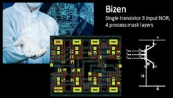
The term "quantum junction transistors" (QJTs) may conjure images of dilithium crystals, flux capacitors, and other imaginary power technologies, but an early demonstration run of Nottingham-based Search For The Next's (SFN) unique "Bizen" wafer process technology has moved the devices from the realm of science fiction to science fact. In fact, the results appear to be so promising that, if SFN can replicate the results in its production devices, they could pose some very real competition to conventional silicon and wide-bandgap (WBG) power devices.
In case you missed the introduction to SFN’s QJT technology we published back in June, the process referred to as “Bizen” is based on the principles of quantum-tunnel mechanics. According to SFN, it can be used to dramatically improve the performance and producibility of any digital or analog semiconductor device.
Fabrication
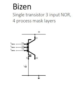
The Bizen fabrication cycle uses standard silicon substrates on conventional, larger-geometry silicon processing lines, but requires only half the process layers of a conventional device. SFN says that eliminating these steps cuts the 15 weeks it takes to process a typical wafer full of CMOS devices to just three weeks. SFN also claimed that chips fabricated in the new process would deliver significant improvements in speed and power, along with a three-fold increase in gate density that enables a comparable QFN device to be fabricated on 1/3 of the silicon real estate.
Since our article ran, those claims were validated when SFN produced and evaluated an undisclosed number of wafers containing QJT devices. At the time of this writing, details of the wafer tests weren’t available. However, the company said that the data they collected demonstrated the silicon-based transistors deliver the same voltage levels, switching speeds, and power-handling performance normally associated with devices fabricated using more exotic WBG materials. The wafer tests also show that the Bizen process can produce QJTs that are able to support operating voltages of up to 1,200 V, very low conductive losses, and an effective current gain of over 1 million.
Assuming the tests are as successful as SFN's announcement would lead us to believe, they validate the company's plans for its first commercial application of the technology—a family of Bizen QJT power devices. The family will include three parts rated at 1200 V/75 A, 900 V/75 A and 650 V/32 A, available in standard TO-247 or TO-263 power MOSFET packages. SFN also released other comparative performance metrics for an even more powerful device on its short-term roadmap—a 1200-V/100-A QJT, also in housed in a TO-247 package. The losses at rated current will be one quarter (Integration Intensified
Another unique aspect of the Bizen process is its ability to allow power transistors and digital logic circuits to be integrated on the same device. David Summerland, CEO and founder of SFN, says, “The QJT is the first power device on the Bizen family roadmap. This will shortly lead to the PJT (processor junction transistor), an integrated Bizen device with its own processor that can also be produced on a manufacturing cycle time of eight days, heralding a new era of intelligent power devices. The technology will also enable direct connection between the 1200-V/5-A QJT power transistor and a low-voltage, low-current CPU output port such as a PWM.”
Summerland contends that, once commercialized, QJTs will have several technical and economic advantages over conventional silicon and WBG power devices. “To get this level of performance from traditional silicon-based MOSFETs, the device size must be much bigger. 1200 V/7 5A in a TO-247 housing can be achieved using wide-bandgap materials like silicon carbide, but this approach has other well-known issues.
“SiC, for example, takes much longer to process and has a significant manufacturing carbon footprint. Also, regardless of the roadmaps, SiC does not scale like silicon, and the economic argument that SiC can match silicon does not take into account the advances made possible by Bizen. By contrast, the data we have obtained from physical wafer tests proves that by using Bizen on silicon substrates, our QJTs deliver the same performance as SiC or GaN."
Additional details about Bizen and SFN are available at Search For The Next's web site and at https://www.wafertrain.com/blog.