Designing a Modern Hardware Emulation Platform
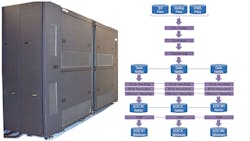
Unlike other electronic-design-automation (EDA) point tools, developing a hardware emulation for functional verification requires mastering multiple disciplines. Depending on the architecture of the emulator, it involves five disciplines (Fig. 1).
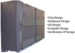
The EDA industry assists all four or five technological fields with dedicated point tools. To create a leading-edge emulation system, developers must approach all fields as a tightly integrated solution.
Before exploring the disciplines, let’s review the architectures of today’s hardware emulators built on one of three types of re-programmable devices. Two consist of custom-made silicon devices. The third uses commercial field-programmable gate arrays (FPGAs). They are:
- Custom processor-based emulator
- Custom emulator-on-chip (EOC)-based emulator
- Commercial FPGA-based emulator
While principles of operation of the three approaches fall beyond the scope of this article, one functional aspect has an impact on the device-under-test (DUT) compiler development. In a processor-based emulator, similar to the workings of a hardware-description-language (HDL) simulator, the DUT is compiled into a data structure, stored in memory that the emulator’s Boolean processors evaluate during run-time. In EOC-based and FPGA-based emulators, the DUT is mapped into a gate-for-gate silicon fabric.
Designing the Hardware
Developing a hardware emulation platform is a major project. It must accommodate a wide range of DUT complexities ranging from a few million ASIC-equivalent gates to well over 10 billion gates. It maps a DUT topology that may be driven by many thousands or millions of complex clock trees, fed by a multitude of asynchronous primary clocks. It ought to lodge large banks of complex memories and intellectual-property (IP) blocks and serve extensive I/O connectivity.
From the bottom-up, the process involves printed-circuit-board (PCB) design populated with re-programmable devices tasked with mapping the DUT, DUT embedded memories, DUT debug memories for collecting DUT activity during run-time, and auxiliary components.
Moving up the hierarchy, the undertaking includes the design of racks hosting PCBs and cabinets to accommodate the racks. High-capacity power supplies and robust cooling systems complete the hardware design job. Depending on the type of emulator, cooling systems can either be based on forced air or fluid circulation.
To achieve scalability and expand design capacity into several billions of gates, multiple interconnected cabinets are necessary. The driving criteria is to design a monolithic cabinet with the largest design capacity possible to reduce the number of cabinets needed to reach the greatest capacity.
Particularly critical is the hierarchical network interconnecting re-programmable devices, extending from the PCB to racks and cabinets. The network should ensure sufficient routing resources to emulate a wide range of designs at a high speed of execution.
An overall design objective calls for keeping power consumption to a minimum to minimize cost of ownership and ensure high reliability. That means calculating the amount of energy feeding the ventilation and air-conditioning system, with dimensions and weight of the emulation platform.
All make the case for mastering the art of hardware design mandatory to create a state-of-the-art hardware emulator.
Designing the Re-programmable Devices
As mentioned earlier, today’s vendors select one of three different technologies. Two use custom-made and one uses off-the-shelf chips, traditionally provided by Xilinx (see table).

The two custom-made architectures have been validated by multiple generations of devices over the past 20 years, supporting the development of new generations of chips for the foreseeable future.
At the time of this writing, the three approaches are implemented on different semiconductor process nodes, albeit not the latest. Yet, designing silicon at advanced process nodes is time-consuming and expensive, and requires an uncommon and highly qualified set of skills, not to mention exceptional talent.
Based on historical data, emulation system development for custom chip-based systems requires approximately four to five years.
Creating the DUT Compiler
The first step in deploying an emulation platform involves mapping the DUT onto the emulator’s re-programmable resources via the compilation process.
While the team creating the hardware portion of an emulator may include 10 to 20 hardware developers and, possibly, a similar number of semiconductor designers, the team designing the compiler can comprise up to 100 software designers. The emulator compiler absorbs the largest slice of the R&D personnel budget. Let’s consider what’s required.
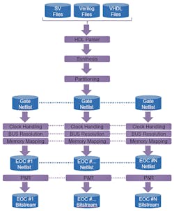
The emulator compiler harnesses a set of technologies, more for the FPGA-based and EOC-based platforms than for the processor-based version. For the former, the main compilation tasks include register-transfer-level (RTL) synthesis, netlist partitioning, timing analysis, clock mapping, memory mapping, board routing, and FPGA or EOC placing and routing (P&R). In the processor-based emulator, re-programmable chip P&R is replaced by scheduling computations on Boolean processors.
It begins with parsing the DUT description using any combination of Verilog, VHDL, or SystemVerilog HDLs. The RTL code is synthesized into a structural netlist.
Since the goal of RTL compilation for an emulator is purely functional, various aspects of synthesis relevant to optimization for physical implementation can be omitted to facilitate faster compilation. Optimizations to logic primitive count and netlist depth are still appropriate to provide a final compilation result with the best capacity and performance characteristics. Emulation system providers typically use custom-developed synthesis technology with these characteristics.
Once the DUT netlist is generated, the compilation flow diverges depending on the emulation technology. In FPGA-based and EOC-based platforms, the gate-level netlist gets partitioned across an array of re-programmable devices implementing the DUT.
In splitting the netlist, a less-than-perfect partitioner may assign uneven blocks of logic to one or more re-programmable devices, causing interconnect congestion despite the use of modern GHz+ rates of data transport in the emulator network. Likewise, a partitioner that doesn’t handle timing may introduce long critical paths on combinational signals by routing them through multiple chips, called hops, detrimental to the maximum speed of emulation. Here, an accurate timing analysis tool can identify such long critical paths and avoid hops.
The impact on the emulation speed associated with partitioning can be dramatic. This partitioning technology is unique, and the tool is typically developed from scratch.
The need to map clocks raises an even greater challenge. Modern designs can use hundreds of thousands of derived clocks distributed over hundreds of re-programmable devices. Designers reduce power consumption by using complex clock-gating strategies. Effort goes into the compiler’s ability to efficiently manage these clocks.
After all this is done, re-programmable devices must be placed and routed. The P&R tool is either supplied by the off-the-shelf FPGA vendor or created by the EOC vendor.
In the processor-based emulator, the compiler partitions the DUT among processors and schedules individual Boolean operations in time steps. The compiler doesn't have to deal with P&R and instead deals with allocation of computations to specific Boolean processors and timeslots.
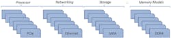
DUT memories in all emulation systems are implemented via memory models. These configure the on-device memory resources and on-board standard memory chips to act as ASIC memories of various shapes and sizes, as well as other specialized memory devices like DDR3 SDRAM, GDDR5, and SDRAM. For this article, the creation of memory models falls under the “Creating the Supporting Environment” section further down.
Compiling a design is a computationally intensive process, dependent on design size and complexity. To speed up the undertaking, the process is heavily parallelized in multiple threads that can run concurrently on PC farms. This parallelization adds another dimension to the already difficult mission to design a compiler (Fig. 2).
An emulator’s compiler requires leading-edge synthesis, partitioning, timing analysis, clock mapping, and P&R technologies, compounded by the need to be heavily parallelized. It’s no wonder that it takes so much attention from the R&D team.
Designing the Emulation Run-Time OS
Once the DUT is mapped onto the emulation platform, it’s ready to be evaluated and debugged, which is accomplished by run-time software or the emulator’s operating system.
The run-time software’s development team, smaller in size than that of the compiler, deals with the environment that drives the DUT. It applies the stimulus; collects and processes the response; and handles all collaterals, including SystemVerilog assertions (SVAs), monitors, and checkers required to control and debug the DUT. It also captures the design activity necessary to trace a design bug.
Run-time software embraces two different components. The first is tasked with evaluating the DUT combining the operating system and software running in one or more host computer systems and extensive firmware loaded in the emulator. The two manage input/output operations of the DUT mapped inside the platform and give users the ability to start, stop, rewind, loop, single-step, save, and restore all typical run-time tasks.
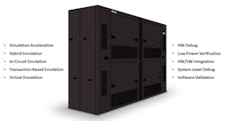
Unlike a modern emulator’s forerunners deployed in only one operational mode called in-circuit emulation (ICE), today’s emulators can be deployed in multiple modes of operation. Beside ICE mode, they can be deployed in acceleration mode, which can be further divided in two sub-classes: cycle-based acceleration—not popular because of the limited speed up versus an HDL simulator—and transaction-based acceleration. The untimed, transaction mode initiated the use of the emulator in a virtual environment and the ability to run software on a virtual platform.
Run-time software that controls the emulator must support all of the above and is intimately tied with the operation of the design itself. It deals with any real-time issues or virtualization layers that might be required to make the hardware and processing elements available to the applications that will ultimately be visible to the system user (Fig. 3).
The second component of run-time software consists of the DUT debugger. Unlike debugging a design in a logic simulator, where total design visibility and controllability is natively ensured by the tool’s software algorithm, debugging in an emulation system requires the creation of a DUT’s internal visibility and controllability at run-time.
Visibility and controllability can be built in the silicon fabric of the re-programmable elements or at compile time via the insertion of probes or dedicated instrumentations, or often some combination of the two. In all cases, visibility and controllability are managed by the debugger.
The debugger must efficiently manage data capture at run-time and support all modern debugging means such as SVAs, checkers, monitors, and coverage. Since an emulator can handle billions of gates’ worth of functionality spanning billions of verification cycles, a more comprehensive debugger is unlikely to be found anywhere else.
Creating the Supporting Verification Environment
Building an ecosystem in support of an emulator involves multiple aspects, some of them related to the DUT, others to the test environment.
Any DUT, especially large DUTs, include substantial embedded memories modeled to be mapped inside the emulator. Creating memory models, while not a major project per se, requires a specific level of expertise.
When an emulator is deployed in virtual mode, the interface between the DUT and the virtual environment can be modeled via a VIP that implements a communication protocol, called a transactor. Specifics of each transactor depend on the application.
Transactors for the most popular protocols, such as PCIe, USB, and Ethernet, are provided by emulation or third-party vendors. Their creation requires IP design skills and specialization in specific vertical markets, such as communication or networking. Emulator users may need custom transactors as well if their designs use proprietary protocols.
A third category of emulation VIP includes speed adapters consisting of electronic boards that act as FIFOs when the emulator is deployed in ICE mode. Real target systems typically run at multi-gigahertz rates, several orders of magnitude faster than the speed of the emulator. The insertion of speed adapters between each emulator IO and the target system guarantees that the two clock domains communicate without data losses or protocol violations (Fig. 4).
Conclusions
To create a leading-edge emulation system, the development team must address at least four or five technological domains of the design automation know-how and draw from widely disparate technological fields. It must do so to ensure all elements of an emulator work together cohesively.
For an emulator to be competitive, all technologies must perform flawlessly with little room for error. The weakest link becomes the platform’s limitation.
Charley Selvidge, Ph.D., is chief architect and senior director of R&D for the hardware emulation business at Mentor, a Siemens Business.
Dr. Lauro Rizzatti is a verification consultant and industry expert on hardware emulation. Previously, Dr. Rizzatti held positions in management, product marketing, technical marketing and engineering.
About the Author
Charley Selvidge
Lead Architect for Veloce, Mentor, a Siemens Business
Charley Selvidge, Ph.D., is chief architect and senior director of R&D for the hardware emulation business at Mentor, a Siemens Business.

Lauro Rizzatti
Business Advisor to VSORA
Lauro Rizzatti is a business advisor to VSORA, an innovative startup offering silicon IP solutions and silicon chips, and a noted verification consultant and industry expert on hardware emulation. Previously, he held positions in management, product marketing, technical marketing and engineering.
Comment About the Article
To join the conversation, and become an exclusive member of Electronic Design, create an account today!

Leaders relevant to this article: