Emulation-Centric Power Analysis of SoC Designs
Download this article in PDF format.
What you'll learn:
- How FinFET technology has changed power-consumption analysis.
- Steps involved in taking a hierarchical approach to performing proper power analysis.
Verification expert Lauro Rizzatti recently interviewed Jean-Marie Brunet, senior marketing director, Scalable Verification Solutions Division (SVSD), Siemens EDA, about the importance of accurate power estimation and optimization for system-on-chip (SoC) designs.
What is the problem facing the semiconductor industry today regarding pre-silicon power estimation?
The problem is the discrepancy between estimated pre-silicon dynamic power consumption in SoC designs and actual power dissipated by the manufactured SoC. Over the past several years, customers noticed that when newly designed SoCs were plugged into the sockets of end products, the actual dynamic power consumption exceeded the estimated power by an order of magnitude.
It has become critical to accurately predict real power consumption while designing and verifying new designs.
The main cause for the discrepancy is the switch from traditional planar CMOS to FinFET semiconductor technology. Historically, the traditional CMOS technology suffered significant standby or static current leakage. Moving to lower nodes, below 32 nm, the standby current grew exponentially and became unmanageable. FinFET technology drastically lowered the static current. Unfortunately, it did not meaningfully change the switching or dynamic current.
Can you expand a bit on dynamic power dissipation in FinFETs?
The FinFET transistor drastically alleviates the power leakage of planar devices via a 3D approach. By raising the channel and wrapping the gate around it, the resulting structure provides a more efficient channel control that decreases threshold and supply voltages (Fig. 1).
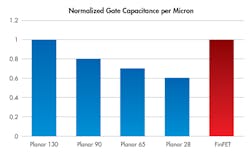
In FinFETs, dynamic power consumption makes up most of the total power dissipation because of higher pin capacitances compared to planar transistors. This results in higher dynamic power numbers.
Designing with FinFET technology requires more stringent design rules that take into account FinFET process requirements. The new rules curb synthesis, placement, floorplanning, and optimization affecting design metrics.
RTL-level power analysis is now mandatory, must start early in the design flow, and be carried out at all stages of the design flow, concurrently with other design metrics, such as performance and area. Cross-probing between RTL, embedded software code, and layout is essential to identify and debug problems early in the design flow.
What other problems contribute to the discrepancy between estimated pre-silicon dynamic power consumption?
Another important issue comes from the intrinsic limitations of the stimulus exercising the design under test (DUT) during pre-silicon design verification.
Today, the electronic industry makes heavy use of benchmarks to gauge performance and power consumption of new designs. Different industry segments use different types of benchmarks.
In the mobile industry, a very popular benchmark called AnTuTu evaluates the performance/power of smartphones and tablets devices. For GPU-centric design, the most popular are Car Chase, Manhattan, and all of the Kishonti benchmarks.
In the artificial-intelligence/machine-learning (AI/ML) industry, the MLPerf benchmark suite measures performance/power of ML software frameworks, ML hardware accelerators, and ML cloud platforms. It is popular for both training and inference. In storage, measuring IOPs provides an accurate evaluation of performance/accuracy for new devices.
It is imperative to run these benchmarks in pre-silicon validation. The full visibility into the design can identify areas of excessive power consumption way before silicon is manufactured and allow for design corrections.
How do you measure power consumption in pre-silicon validation?
Traditionally, power consumption has been accomplished at the gate level by tracking the switching activity of the DUT exercised by testbenches consisting of regression vectors. The approach has two problems.
First, the testing happens very late in the design cycle. Although the discrepancy with silicon is within only 5%, there is not enough flexibility to correct the problem in the design. A better compromise is to evaluate dynamic power consumption at RTL that leads to a larger deviation from silicon in the ballpark of 15%, but provides higher flexibility to support design changes.
Second, testbench vectors are not a good representation of how the design is going to be used. To achieve accurate power estimation, it is important to capture the switching activity as accurately as possible in the context of the target system running real-life workloads and performance/power benchmarks, as described earlier.
What is the setup to perform power analysis, and how do you accomplish it?
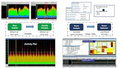
Obviously, RTL simulation cannot undertake the demanding job anymore. What’s needed is a hierarchical approach, starting at the high-level of design abstraction and moving in stages all the way to RTL and the gate level. No single tool can do the entire job any longer. Instead, multiple tools with optimum tradeoffs of characteristics can accelerate power estimation and optimization (see table below).
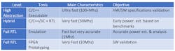
In the first step, the entire DUT described in C/C++ at high abstraction level is quickly validated against hardware/software specifications, and very rough power consumption is estimated.
Next, power dissipation is validated in a hybrid setup consisting of a design portion described at a high-level of abstraction, typically including processing cores and memories such as Arm Fast Models, and the other design portion at RTL. The high-level of abstraction section is run on a host server, the RTL is executed on a hardware emulator, and the two are connected via a transaction-based interface.
While the emulator runs at a speed of very few megahertz, the hybrid configuration may achieve speeds in the ballpark of 50 MHz—fast enough to quickly boot Android, Linux, and all of the kernel underneath, as well as execute benchmarks and real-life applications.
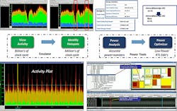
The setup provides a head start to profile the entire design for power consumption in a relatively short time. By plotting the switching activity over a long run of billions of clock cycles, the design team can identify hotspots of high- and low-power dissipations in ranges of a few million clock cycles. Similarly, by tiling power-dissipation areas in an activity map, the team can visually identify design sections of high and low power dissipation.
Once hotspots and critical tiles are pinpointed, the team can switch to full RTL and enjoy accurate and detailed visibility into each design net. By correlating the activity plot to the embedded software code as well as the activity map to the RTL code, the team can rapidly zoom in on areas of potential power problems.
It’s extremely important to capture the complete design activity for the entire workload processing, and avoid sampling, which is typically done with FPGA-based platforms that lack full internal visibility (Fig. 2).
It’s worth mentioning that a major semiconductor house had a change of heart about early power profiling at RTL after witnessing the execution of the Angry Birds benchmark on one of its SoCs running on an emulator. I had to chuckle thinking that my daughter entertains herself playing Angry Birds on her iPod, and this major semiconductor firm runs the same program on an emulator.
What developments do you anticipate next?
One novel design aspect that is very complex to manage at the pre-silicon stage relates to chiplets, die stacking, and 3D IC packaging.
My previous power profiling and analysis discussion was based on a monolithic design where all components are combined on a single die. What we’re looking at next are designs implemented in a complex 3D IC package. In many of these designs, CPU cores are on one die, GPU cores on another, memories on a third, and so on, and they communicate among themselves via an embedded multi-die interconnect substrate or bridge (EMIB) (Fig. 3).
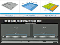
Performing power profiling and analysis as well as thermal analysis on the design hardware hierarchy and the configurable embedded software stack spread over multiple dies is complex and challenging.
We need to conceive modular and hierarchical compilation of a complete design targeting a specific hardware-emulation platform, and devise the ability to browse, identify, and debug hardware/software-based activity through the design hierarchy.
About the Author

Lauro Rizzatti
Business Advisor to VSORA
Lauro Rizzatti is a business advisor to VSORA, an innovative startup offering silicon IP solutions and silicon chips, and a noted verification consultant and industry expert on hardware emulation. Previously, he held positions in management, product marketing, technical marketing and engineering.
Comment About the Article
To join the conversation, and become an exclusive member of Electronic Design, create an account today!

Leaders relevant to this article: