“Digital Twins” and Other Trends Impacting the EDA Space
>> Electronic Design Resources
.. >> Digital Editions
.. .. >> Top Stories of the Week
.. .. .. >> 2021 Electronic Design Forecasts
What you’ll learn:
- Synergies within the EDA industry.
- What is a “digital twin”?
- How are digital twins influencing different EDA technology areas?
The electronic-design-automation (EDA) field remains one of the most competitive and technically challenging with respect to the electronics universe. I spoke with Joe Sawicki, Executive Vice President with Siemens, about this space as well as their new name and where he envisions EDA is headed in the near future.

How does Mentor see the EDA space progressing?
This is an exciting time to be in EDA. Around the globe, almost every industry is redefining themselves through digitalization. And, as you know, the IC is the heart of digitalization.
If you look at the business press these days, it’s rare to not see a mention of digitalization, digital world, digital enterprise, or the digitalization of everything. And I think that’s because companies are looking to leverage semiconductor technology to change their business models, logistics, and finance, driving an incredible opportunity for the semiconductor landscape.
Whether it’s startups or large system houses creating internal design teams, we’re seeing new players in the IC design market every day and it’s clear that will drive tremendous growth in the EDA space.
I understand that Mentor reaches a significant milestone this month?
That’s right. Four years after Siemens announced its intent to acquire Mentor Graphics, “Mentor, a Siemens business”, is now “Siemens EDA,” while remaining a segment of the larger Siemens Digital Industries Software organization. The transition of our brand to Siemens EDA coincides with Mentor’s legal integration into Siemens in the U.S. effective January 2021.
Being a part of Siemens in recent years has allowed us to expand our EDA footprint via significant M&A. In addition, our customers can increasingly pair our EDA portfolio with Siemens technologies for simulation, mechanical design, low-code, manufacturing, and IoT cloud optimization.
When Siemens announced plans to acquire Mentor, some in the IC industry were surprised. Since then, a number of synergies have become increasingly apparent. Of the EDA-IC segment that you lead, what are some of the synergies you might have with the broader Siemens Digital Industries Software organization?
There are quite a few. One notable synergy relates to the trend toward systems companies bringing IC design in-house. This is happening across a number of industries, including the automotive, consumer electronics, and networking markets, just to name a few. Designing custom silicon can help OEMs meet very specific requirements, often resulting in better, highly differentiated end products.
Because systems companies focus as much on the end product as on any particular IC or subsystem, they are key drivers of the increasing convergence of semiconductor design and systems design. That’s a trend of relevance—not just for IC design teams at systems companies, but for all semiconductor design engineers. So, from this perspective, it becomes quite easy to see the synergies between Siemens EDA and the complementary engineering technologies across the broader Siemens Digital Industries Software organization.
One of the ideas that Mentor, which is now under the banner of Siemens EDA, seems to have embraced is the concept of the “digital twin.” What is digital twin technology?
Put simply, it’s leveraging digitalization to generate the best possible virtual representation of a physical world. It allows companies to thoroughly test a virtual model of their product before committing to manufacturing. The concept originated in the mechanical design world decades ago, and many early applications focused on manufacturing and mechanical engineering tasks.
Siemens was a pioneer of the digital twin concept. Today, digital twins are one of the core conceptual models for product-lifecycle-management (PLM) technology. However, the technology is applied to a range of markets in the mechanical design world. We believe that extending that to IC and electronic systems design is a logical next step, since we in the IC design community have essentially been designing and testing this way for decades. In fact, Digital twins are poised to take a giant leap forward by allowing companies to test their IC designs more easily and upfront in the context of the end system.
What does the digital twin mean in the context of IC design?
For IC design engineers with any significant degree of experience, the notion that Digital Twin technology is fundamental to advancing state-of-the-art semiconductor design might seem a given. After all, EDA tools have successfully generated increasingly accurate digital representations of IC designs for more than 35 years.
But designing a modern IC is more challenging than ever. Creating a virtual representation of an IC design is just one of many steps in developing and producing a next-generation SoC.
As manufacturing complexity and demand for ever more advanced technology grows, it has become much more difficult for companies to design, verify, and validate products. So, we believe digital twin technology represents a path toward radically faster and more complete IC verification and validation cycles, paving the way for higher-quality end products and faster time to market.
There’s a greater need than ever to not only verify that IC designs function properly to the IC specification, but also to verify and validate that they work in the context of the end-system. This is particularly the case if the system needs to comply with a particular set of protocols or standards, or if safety and security are mandatory. Increasingly, to do this correctly requires verification and validation technology (e.g., simulation) that moves beyond the traditional realm of what’s been considered EDA and closer to the digital twin concept.
Demand for shorter design cycles and faster time to market has always been central to IC validation and verification. How do you view digital twins in this context?
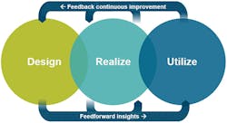
We believe that digital twins represent a “shift left” for IC design, because they allow multiple disciplines to work seamlessly together, eliminating boundaries between electrical and mechanical design teams by providing a single source of truth. They also allow IC designers to verify and validate their devices against highly accurate digital simulations of the subsystems, systems, end products, and even the environments within which ICs will operate throughout their lifecycle. The result is a significant advancement in the verification and validation of ICs.
Another way digital twins shave time off of verification and validation cycles is by providing an environment for modeling different parts of a design across different stages of the maturity cycle. This allows IC designers to test software much earlier in the design process.
Another concept that’s gaining traction in IC design is silicon lifecycle solutions. Where do digital twins fit into that concept, if at all?
Silicon lifecycle technology truly is a game changer. By embedding advanced monitoring hardware into complex SoCs, customers have access to “fab-to-field” analytics capabilities. These can accelerate silicon bring-up, optimize product performance, and confirm that devices are operating “as designed” for functional safety and cybersecurity purposes.
Last summer we announced our acquisition of UltraSoc, a highly regarded pioneer in the field of silicon lifecycle technology. This portfolio is now integrated into our Tessent product line.
Digital twins can serve as a single source of truth for the collection of data that can generate feedback for continuous improvement downstream, as well as feed insights forward. With the product actually operating out in the field, issues can occur. That data can be fed back to the matching digital twin of the design, and then we can use the data to either improve the design, or even send out a software upgrade to the product in the field. So, digital twins and silicon lifecycle technologies are quite synergistic.
Where can our readers learn more about the role of digital twins for IC verification and validation?
I delivered a keynote recently on this topic, and it presents a more detailed overview of the Digital Twin concept for IC design. It’s available on demand at https://ve.on24.com/vshow/Mentor_U2U/.
>> Electronic Design Resources
.. >> Digital Editions
.. .. >> Top Stories of the Week
.. .. .. >> 2021 Electronic Design Forecasts
About the Author

William G. Wong
Senior Content Director - Electronic Design and Microwaves & RF
I am Editor of Electronic Design focusing on embedded, software, and systems. As Senior Content Director, I also manage Microwaves & RF and I work with a great team of editors to provide engineers, programmers, developers and technical managers with interesting and useful articles and videos on a regular basis. Check out our free newsletters to see the latest content.
You can send press releases for new products for possible coverage on the website. I am also interested in receiving contributed articles for publishing on our website. Use our template and send to me along with a signed release form.
Check out my blog, AltEmbedded on Electronic Design, as well as his latest articles on this site that are listed below.
You can visit my social media via these links:
- AltEmbedded on Electronic Design
- Bill Wong on Facebook
- @AltEmbedded on Twitter
- Bill Wong on LinkedIn
I earned a Bachelor of Electrical Engineering at the Georgia Institute of Technology and a Masters in Computer Science from Rutgers University. I still do a bit of programming using everything from C and C++ to Rust and Ada/SPARK. I do a bit of PHP programming for Drupal websites. I have posted a few Drupal modules.
I still get a hand on software and electronic hardware. Some of this can be found on our Kit Close-Up video series. You can also see me on many of our TechXchange Talk videos. I am interested in a range of projects from robotics to artificial intelligence.
Comment About the Article
To join the conversation, and become an exclusive member of Electronic Design, create an account today!

Leaders relevant to this article: