Machine Learning, Neural Net Drive Collimated, On-Chip Nano Light-Beam Design
What you'll learn:
- What prompted the MIT team to research and develop a nanoscale "flashlight"?
- Details on the metasurface that was designed to create the source-beam collimator.
- How a DNN, CNN, and machine learning were applied in the design process.
- Results obtained through testing.
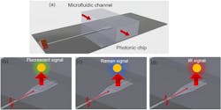
There’s significant interest in on-chip miniaturization of spectroscopic sensing arrangements used in science, biology, and medicine to implement fluorescence imaging/microscopy, infrared (IR) spectroscopy, and Raman spectroscopy (Fig. 1). All are used for quick, accurate, and non-intrusive analysis of gases and liquids.
However, progress has been limited to some extent by lack of suitable light sources, as most of the research has centered on developing on-chip optical detectors while relatively little attention is given to the complementary excitation sources. A large part of the challenge is that the source illumination must be collimated and have a narrow wavelength spectrum, and often be tunable. Consequently, these “single-chip” analyzers still need an external LED or laser as a source, which adds to their complexity, size, and cost.
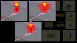
To overcome this barrier, an MIT-based a research team devised and tested a powerful nanoscale “flashlight” on a chip that produces the desired collimated light stream at a specified wavelength. While the fabrication itself used standard microelectronics processes—a big plus, of course—the design approach they used to decide what structures to build on-chip wasn’t standard.
Rather than propose design solutions and then model, simulate, and fine-tune them, they relied extensively on machine-learning techniques. The computer is taught to predict potential solutions using huge amounts of data and the physics of light propagation and manipulation.
They designed a metasurface to create a planar integrated-photonic source-beam collimator for use in on-chip optofluidic sensing applications. Further, to optimize the metasurface to better reach the various performance goals, they used the gradient-descent method with an iterative inverse-design approach.
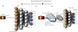
The team started with the end result of the desired diffraction-beam profile, then applied an inverse model to evaluate the optimal design parameters of the metasurface (Fig. 2). Parameters such as the surface repetition period and height and size of scatterers were calculated using a feedforward deep neural network (DNN) and convolutional neural network (CNN) architecture.
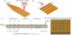
There’s more to this approach than simply defining objectives and having the machine-learning algorithm go through options in an attempt to maximize performance along the desired directions. They note that the gradient-descent method is highly sensitive to initial conditions, so it was critical to initialize the process as accurately as possible. This was done using an effective mirror model for the meta grating structure and a cascaded mirror model with grating grooves (Fig. 3).
The project wasn’t just a theoretical exercise in the use of deep machine learning to devise innovative integrated, high-performance photonic structures. Once an optimal design that met the criteria was established, they fabricated a device using single-layer patterning on a silicon-nitride substrate using e-beam lithography and reactive ion etching to define the geometry of the grating structures.
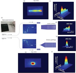
For the test and evaluation phase, the team used a beam profiler and near-infrared (NIR) camera as well as a separate alignment camera to determine the beam dispersion profile (Fig. 4). That was then compared to a conventional beam grating of comparable size (Fig. 5).
Obviously, performance of a device such as this can’t be summarized by a single parameter, nor is it easy to characterize it and then compare it to conventional beam-grating approaches. The researchers note that power delivered through the metasurface was approximately five times that of the conventional grating surface and the 3-dB width of the beam spot increased from 100 μm to ~300 μm with the metasurface, for footprint of 200 × 50 μm2. This enables greater light illumination efficiency of the on-chip device.
The team concludes that this type of excitation source, when integrated with a planar waveguide-based photonic detector/photodetector, has the potential to miniaturize optical spectroscopy and accelerate medical sensing. Due to the dual aspects of the project—the device itself and its machine-learning design approach—the work is described in two papers published in Nature Scientific Reports, “Inverse design of photonic meta‑structure for beam collimation in on‑chip sensing” and “Design of optical meta‑structures with applications to beam engineering using deep learning.” The papers discuss all aspects of the project, from theory to conception, through execution, ML flowcharts, actual fabrication and test, along with the requisite optical physics and associated equations.
About the Author

Bill Schweber
Contributing Editor
Bill Schweber is an electronics engineer who has written three textbooks on electronic communications systems, as well as hundreds of technical articles, opinion columns, and product features. In past roles, he worked as a technical website manager for multiple topic-specific sites for EE Times, as well as both the Executive Editor and Analog Editor at EDN.
At Analog Devices Inc., Bill was in marketing communications (public relations). As a result, he has been on both sides of the technical PR function, presenting company products, stories, and messages to the media and also as the recipient of these.
Prior to the MarCom role at Analog, Bill was associate editor of their respected technical journal and worked in their product marketing and applications engineering groups. Before those roles, he was at Instron Corp., doing hands-on analog- and power-circuit design and systems integration for materials-testing machine controls.
Bill has an MSEE (Univ. of Mass) and BSEE (Columbia Univ.), is a Registered Professional Engineer, and holds an Advanced Class amateur radio license. He has also planned, written, and presented online courses on a variety of engineering topics, including MOSFET basics, ADC selection, and driving LEDs.
