Overcome Mechanical Constraints to Balance PCB Design Functionality

This article is part of the TechXchange: PCB Tools and Technology
Members can download this article in PDF format.
What you’ll learn:
- The connection between mechanical and electrical concepts
- How to fit many components into a limited space.
Proper communication is necessary when creating products in a team with diverse backgrounds. Disclosing the product requirements to other team members early raises your chances of establishing conflicting design issues and solving them while still in the schematic stage. In turn, the design process becomes a cost-effective, flawless, and less time-consuming exercise.
If you have clear and practical electronic requirements, you can quickly formulate early mechanical and electrical designs. Cover limitations and industrial design will shape the mechanical design of your project. Other factors like ergonomics, industry guidelines, and standards also will play a role.
When mechanical personnel receive a practical working plan and electrical personnel have a working schematic, you can create your printed-circuit-board (PCB) design.
PCB Outline and Keepouts
The initial step in creating a PCB design is approving the first circuit board outline. This will enable you to agree on the board size and shape early in the process. A mechanical expert should create a sketch containing the PCB outline, regions with height limits, components, and trace keepouts.
The PCB outline represents the final shape after manufacturing, and it relies on the mechanical aspect of the board. The mechanical engineer can start by creating a sketch containing the largest board size, considering the projected points in the mechanical plan. The mechanical engineer collaborates with the electrical engineer to minimize the board outline to the smallest possible measurement, reducing substrate costs.
Remember, rectangular PCB outlines are more cost-effective than curved outlines due to the minimal substrate waste and little manual work in routing the shape. Therefore, when sharing your PCB outline with other members, it includes the highest height limit for electrical parts. Mostly, the highest height constraint differs across the board because of mechanical limitations.
Your sketch should highlight the PCB points with height constraints that are lesser than the highest limit to prevent interference hitches during PCB assembly. Component keepouts are regions where the mechanical shape touches the board or is so close that there’s an inadequate allowance for small parts. You should notify other team members about these regions as was the case with height constraints.
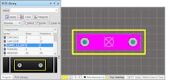
Figure 1 shows an All Layer keepout integrated to confine all parts, except tracks. This facilitates net connections in layouts where such components are applied, while limiting the close mounting of other parts.
Lastly, the trace keepouts are board regions in any layer that lack traces. For mechanical engineers, the primary concerns at this stage are areas with metal components positioned close to the board, mounting structures, and board edges (e.g., inner cutouts). Ensure you leave a small space from the PCB edge with no trace to inhibit electrical arcing. This space is determined by the voltage, current, and Dk value of the board substrate.
If your electronics needs regulatory certification by a local agency, you should follow their guidelines to avoid future problems. But, generally, start with the IPC-9592B standards. Remember to create additional keepout distance to accommodate the size of the screw head when dealing with metal hardware.
Layout
At this stage, the electrical engineer can start creating traces that join electrical parts on the board. It’s recommended to categorize the parts into joints with no height constraints before relocating them into constrained sections. Mechanical and electrical engineers should partner to establish large, unusual, and high-risk parts.
Of course, care should be taken when laying out these components—the entire team should appraise the specification document. You should mold the components in CAD to ensure they fit well with the mechanical design. Some layout regions, like ac and dc circuits, limit component placement.
When you finish creating the design, the PCB software you’re using will export it in a three-dimensional format, which is essential when parts are closely mounted. The mechanical specialist should transfer the format into the mechanical format for assessment. If the whole team approves the design and perfectly fits into one board, your design is successful and ready to move into the manufacturing phase.
Fitting Several Components into an Inadequate Space
The surface area is an essential part of a PCB layout. At first, you will realize that there’s lots of space to mount components. However, as connectivity becomes denser, that space disappears to the point where it becomes difficult to fit all required devices onto the board. You can overcome this issue through various techniques such as:
Adding more layers to the board
In this scenario, you have sufficient space to mount all your devices. Still, when the electrical engineer routes the traces and creates the necessary distance to inhibit arcing, the area becomes limited. The best option is adding more board layers, though it will increase the cost. Most boards have between one to eight layers, but you can add more layers to accommodate your components.
Creating daughter PCBs
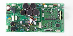
When experiencing space constraints on your primary board, the motherboard, you can relocate a complete circuit onto a new board—the daughter PCB. This will minimize the number of necessary links on the main board and increase the assembly cost because of the additional board. Your assembly also will become more complex due to the new way of accommodating the extra board in your mechanical structure and linking it to the primary board. Figure 2 shows how a daughterboard is connected to a motherboard.
Nevertheless, this is still an ideal solution since it’s easy to design a circuit board with reliable placement structures and off-the-shelf mechanisms of linking the daughterboard to the motherboard.
Moving big parts off the board
A situation may arise where significant parts like capacitors and inductors inhibit you from creating a miniaturized and dense board. In such cases, you can’t add more layers or create a daughterboard. The best solution is to move large components off the board in order to free it up.
Create customized placement structures to hold large parts within your package in injection molds. Then, link them with the board using leads.
Linking everything together
If you created space via a daughterboard, the circuits must be linked together in a reliable and low-cost manner. You can use a horizontal or vertical header if a dense circuit system is needed between the motherboard and the daughterboard. If the design rejects the use of headers, you can still use a customized cable assembly.
When space limitations offset cost limitations, the ideal solution is to use a flexible connector or PCB. Instead of applying fiberglass as the base material, a flexible PCB uses Kapton material. This allows users to bend and fold it as they want.
Like in the case of cables, flexible PCBs are customized and low cost when produced in high volumes. However, low-volume production runs are costly due to the equipment that produces the shapes. You can solder flexible connections directly to the board or utilize zero-insertion-force (ZIF) connectors.
Conclusion
Balancing functionality in the context of mechanical constraints in PCB designs is shaped by various considerations. If you manage to detect and solve spatial limits early, you will reduce the number of prototypes it takes to create a functioning product. Cost and performance should be your main concerns when components fail to fit perfectly into the board. Hopefully, this article has enriched your memory, and you will be more creative in your next PCB project.
About the Author
Linda Liu
Overseas Market Manager, MKTPCB
Linda Liu is the overseas marketing manager for MKTPCB, a leading PCB manufacturer that offers high-quality PCB products and services. Since 2012, she has established “first-of-its-kind” industry-changing and transformational business initiatives that increased revenue growth, brand exposur,e and market expansion for MKTPCB. Linda graduated from Western University with a Bachelor’s degree in marketing.
Comment About the Article
To join the conversation, and become an exclusive member of Electronic Design, create an account today!

Leaders relevant to this article: