Wafer-Level High-Power Device Testing
Keeping an IC cool takes on new meaning when power dissipation exceeds 150 watts.
Innovative electrical and mechanical solutions to new wafer testing challenges continue to be developed. For example, the need to position large quantities of contacts very close to each other is being approached through micro electro-mechanical system (MEMS)-based probing. Nevertheless, a number of innovative applications of probe needles continue to demonstrate this well-established technology's resilience. And, with 150-W ICs a reality, the provision and dissipation of large amounts of power also are being addressed.
Naturally, test technology must follow IC process changes. For example, the stack-up of many layers of low-k dielectric isn't as strong as a stack-up of SiO2 layers. As a result, the effects of small probe-card imperfections may become more critical. Solutions have been proposed for both parts of the problem: more flexible cantilever probes that exert less force and increased strength in the device contact area.
Another IC trend has been toward lower core voltages. Although power-dissipation gains certainly have been made by operating at lower voltage, enhanced chip performance generally does use more power. For example, the power dissipation of Pentium 4 ICs increased by more than 30 W as the clock rate went from 2.2 GHz to 3.4 GHz. Similarly, current increased by 30 A over the same change in speed.
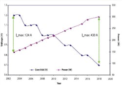
It's not just the size of the increases in current and power that concern wafer-testing professionals. The absolute current now is up to 100 A and predicted to be more than 200 A as the core voltage decreases from the present 1.2 V to about 1.0 V in 2010 (Figure 1).
Power to the Chip
Improvements to the way power is supplied were discussed in Power Delivery Challenges of High Power Logic Device at Sort,• a paper presented at the 2004 SouthWest Test Workshop (SWTW) and written by S. Mobin and K. Zhu, both from Intel. The authors divided the probe-card power path into its constituent parts: the power supply itself, the PCB, the space transformer, the probes, and the probe-to-DUT contact. For each part, an equivalent lumped-constant circuit was developed. Several comparisons of simulated and actual performance verified the appropriateness of the circuit models and values that were used.
To grasp the scale of the high-current testing problem, consider an IC that draws 65 A and has 400 pins devoted to Vcc. If each of the probes delivering power to the IC pads has a 0.5-Ω contact resistance, then the overall parallel resistance will be 1.25 mΩ, and the Vcc drop just due to probe contact IR losses will be 81.25 mV. There are other IR losses not considered, but even if they brought the total drop to only 100 mV, that represents 8% of a nominal 1.2-V supply.
The problem locally is worse because current isn't drawn equally by all 400 pins. Examples used in the Mobin and Zhu paper showed that because one type of circuit used more current than another, memory areas and core logic areas had supply voltages that were 6% different. In addition, because the current varies dynamically, the various inductances throughout the power distribution path contribute to transient droops of as much as 16% of Vcc in response to sudden current changes.
Solutions the authors suggest can be considered good design guidelines rather than revolutionary concepts. They include the use of power planes and vias for high-current power distribution, reduced space transformer R and L, and improved probes with lower inherent L and R as well as lower contact R. Low equivalent series inductance (ESL) and equivalent series resistance (ESR) capacitors to decouple the power supply also will help reduce transient-related droop.
These suggestions, if followed, will reduce voltage droop at the DUT. However, after the space transformer has been made thinner to achieve lower R and L and after better probes have been developed and designed into a probe card, only a short period of relief may have been bought. As chip current continues to increase, similar problems to those addressed in the Mobin and Zhu paper will reappear but at a different scale.
The power-delivery subject was further considered in an SWTW 2005 paper titled Power Delivery Model of Test Probe Cards• by H. Kilicaslan and B. Tunaboylu from Kulicke & Soffa Industries. Sections of the power-delivery path were modeled and analyzed in detail, and the conclusions reached were similar to those of Mobin and Zhu. A 20-A/ns transient current step was shown to produce a 72% droop before design improvements were made. After optimization of the space transformer thickness and addition of suitable decoupling capacitors, the droop was reduced to 45%.
New technologies the paper reported on included reduced-height probes with less L, lower probe-to-DUT contact resistance through the use of better probe tip design and material, capacitors integrated close to probe tips to compensate for the probe L, and a fast transient feedback voltage regulator to reduce fluctuations at the DUT.
Even when hundreds of probes provide power and ground connections to an IC, the very large total current and its unequal distribution mean that one or more probes may be forced to carry a large current. This situation leads to consideration of just how much current a probe can carry safely.
In the SWTW 2005 paper SIU Probe Burn Control• by M. Claudius from Intel, this concern about sort interface unit (SIU) probe damage is rephrased as low-current probes get themselves into high-current trouble.• Without some form of current limiting, a short on an IC power line can cause several amps to flow through a probe, burning the tip.
To determine actual current limits for representative probes, a number of FormFactor MicroSprings• were tested. Although two types of tests were performed one applying current for 5 s with 0.75 s between each application and the other applying a single 17-ms pulse the results were similar. The maximum current that did not damage the probe was found to be about 1.7 A.
As a result, the solution proposed in the paper was to add sufficient resistance in each power probe circuit to limit current to 1.7 A in the event of a shorted DUT. Of course, this solution will limit the achievable current slew rate depending on the probe circuit's L and C components. A more complex but less intrusive means of protecting the probe tips would be a form of electronic current limiting.
Vertical Goes Power: Multi-Site Wafer Probing of Automotive ICs,• an SWTW 2004 paper by R. Gaggl with T.I.P.S. Messtechnik GmbH, Austria, set out to investigate the use of vertical probes in automotive power/logic device testing. Cantilever probes with tips sized according to current requirements previously had been used for this purpose. One goal of the paper was to determine if vertical probes could be used despite conventional wisdom to the contrary.
Dr. Gaggl found that, although vertical probes traditionally were associated with low-power applications, it was not the probe that limited the current that could be applied to any one device pad. Rather, the localized heating associated with the probe-to-pad contact resistance and short, high-current pulses were the limiting factors. In fact, bonding pads could melt if precautions were not taken.
It's interesting to note that a probe tip was not necessarily damaged by the first pulse that caused a bond pad to melt. The thermal mass of each part of the system and the thermal resistances separating them determine the temperature rises caused by an amount of added heat.
For example, in the development of thermal-writing print heads, burned-out elements occurred although the rms current was well within specification. The elements burned out because of high current peaks that caused the internal, low thermal-mass heating element to burn out before producing an excessive temperature rise on the outside of the writing stylus.
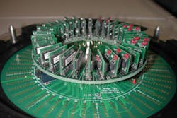
The solution devised by Dr. Gaggl was the SmartClamp module that limited the peak current any one probe could provide but was otherwise transparent to current flow. Figure 2 shows a vertical probe card with added SmartClamp overcurrent protection the ring of small square PCBs. Although not a major consideration in developing the SmartClamp, such a current-limiting approach also protects probes should a DUT have power supply pads shorted to ground.
Getting Power Out of the Chip
For low-power devices, a thermal chuck provides a constant-temperature environment. All the devices on a wafer are held close to the same temperature with variations attributed to the thermal chuck limitations. Because only a small amount of power is involved, dynamic changes within each device, even in a multiple-DUT test setup, have little effect.
The situation is completely different for high-power devices. Testing these requires a thermal chuck to sink large amounts of power while maintaining a constant temperature. In effect, what's wanted is a thermal resistance value of zero: Regardless of the amount of heat sunk by the chuck, its temperature doesn t change. This isn't possible, but manufacturers have refined chuck designs to achieve a very low thermal resistance below 0.1 C/W.
In an approach analogous to that used to analyze the power supply-to-DUT electrical current path, a heat-flow circuit accounts for temperature drops from the DUT to the wafer back surface, across the wafer-to-chuck interface, and from the chuck surface to the temperature sensor. In addition, because of the close proximity of the various parts of the test system, there is some influence from heat dissipated on the probe board. Of all these losses, the greatest temperature drop is across the wafer-to-chuck interface because of the imperfect contact between the two surfaces.
This interface, then, has become the focus of efforts to improve thermal chuck performance. An SWTW 2005 paper by H. Ibele from Maccs LLC and K. Reitinger from ERS GmbH concentrated on improving the smoothness of both surfaces to maximize heat transfer. ERS GmbH manufactures high-power thermal chucks, and Maccs LLC distributes them in the United States.
The coefficient of thermal resistance of silicon is about 7 C/W per unit area and thickness and that of aluminum about three times less. In other words, if power is dissipated at the rate of 1 W on one surface of a 1-mm silicon cube, that surface temperature will be 7 C higher than the temperature on the opposite face of the cube 1 mm away.
Ibele and Reitinger made several resistive test devices, some as separate chips, some part of a much larger wafer. The devices also contained diodes so that the DUT temperature could be calculated by measuring the diode voltage drop. Each device was mounted on a high-power thermal chuck and the overall coefficient of thermal resistance measured. Figure 3 plots overall coefficient of thermal resistance vs. the length of one side of a square test device.
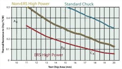
The data points A, B, and C do not fall on a curve corresponding to a constant coefficient of thermal resistance per unit area. Normalized coefficients of thermal resistance found in tables of material constants have units of C-(length)/W.
You calculate the temperature rise of a piece of material through which an amount of power W is flowing by multiplying the coefficient by the length of the material in the direction of the heat flow and dividing by the cross sectional area. The overall K values that Ibele and Reitinger have calculated include the effect of area and length and directly relate temperature rise to power dissipation for the three tests performed.
For the measured data points, applying an equation in which a constant coefficient of thermal resistance has been assumed results in only an approximate fit. This may be because the 21.6 C temperature rise associated with the 100-mm2 chip (case A) is much higher than the 6.1 C rise for the 221-mm2 device (case B). The coefficient of thermal resistance of the silicon close to the hot device would be somewhat different for A compared to B rather than constant.
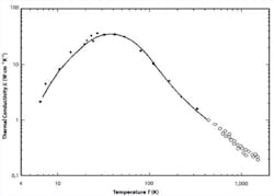
In the region around 25.5 C (298.66 K), the chuck reference temperature used in the tests, the coefficient of thermal conductivity for silicon has a negative temperature coefficient of about -0.001 C-mm/W/ C (Figure 4).1 In other words, instead of remaining constant at 0.149 C-mm/W, for a temperature increase of 21.6 C, it will reduce to 0.128 C-mm/W a change of -14%. For a 6.1 C rise, it will be approximately 0.143 C-mm/W. This means that, for case A compared to case B, the wafer thermal resistance contributed proportionately more to the total device temperature rise.
Also, conditions between cases A and B were different because device A was a separate test chip but device B was integrated into a 300-mm wafer. Although perhaps the effect is small, some heat from device B will diffuse into the surrounding silicon wafer rather than pass directly into the thermal chuck. This effect and the temperature dependence of silicon's coefficient of thermal conductivity mean that temperature drops across the wafer, interface, and chuck cannot be modeled simply by summing three constant thermal resistivities.
In any event, a key element for Ibele and Reitinger in achieving very low overall thermal resistance was good wafer-to-chuck contact. Filling the microscopic voids between wafer and chuck surfaces with helium or a liquid, as other researchers have proposed, was discounted in favor of providing extremely smooth wafer and chuck surfaces. Tests were performed with a probe force of at least 3 kg/100 mm2 or about 43 lb/in.2 to ensure good contact was made.
In contrast, another SWTW 2005 paper described the results of wafer production testing using a liquid interface to a thermal chuck. Liquid Interface at Wafer Test• by P. Diesing, D. Gardell, and D. Audette of IBM Microelectronics focuses on the wafer-to-chuck interface as the largest source of high thermal resistance. Devices already in production demonstrate the steady increase in the heat flux (W/area) that must be sunk by a thermal chuck during device test.

Surface roughness measurements showed the chuck to be flat within 2.9 m across 300 mm with localized roughness of 1.9 m. The surface roughness of a wafer typically was about 0.35 m. In the solution the authors described, a thermally conductive liquid fills the microscopic gaps after the wafer is pulled down onto the chuck by vacuum.
Overall thermal resistance with the liquid interface was an average of 0.13 C/W regardless of the die position on the wafer for a 400-mm2 area die. Test results were lower than those of Ibele and Reitinger at 100 mm2, 0.26 C/W vs. 0.36, but higher for larger die areas.
Summary
As semiconductor device complexity increases, new problems emerge, and finding solutions to previously minor difficulties becomes critical. A range of approaches to many problems was presented at recent SWTW conferences, some only theoretical and others proven in the production environment.
With regard to high-power device testing, detailed research findings have been discussed and contrasted. A degree of continuity among themes can be seen from year to year as significant amounts of work on specific topics accumulates. For example, Ibele and Reitinger referenced a 1998 paper by D. Slaby from Cray Research that described a 20% wafer-to chuck thermal conductivity increase due to filling the wafer-to-chuck interface cavities with helium.
Many of the performance gains reported are incremental but match the demands of projected DUT power dissipation for the next few years. However, it's a good bet that as device power continues upwards, a new test technology will emerge. When it does, SWTW conference papers will address it from angles equally as thought-provoking as those presented here.
References
All of the SWTW conference papers are available at www.swtest.org.
1. Glassbrenner, C. J. and Slack, G. A., Thermal Conductivity of Silicon and Germanium From 3 K to the Melting Point,• Physical Review, Vol. 134, A1058 A1069 (1964) [Issue 4A May 18, 1964].
About the Author
Comment About the Article
To join the conversation, and become an exclusive member of Electronic Design, create an account today!

Leaders relevant to this article: