Testing Written Very Small

By its very nature, microelectromechanical systems (MEMS) testing must cross the electrical/mechanical divide. MEMS devices always include mechanical motion as well as electrical signals, so both aspects are involved in test.
Often, electrical signals are applied that cause motion. For example, a shaft can be turned by successively operating a number of pawls that engage a central toothed wheel. In this case, properly timed pulse trains would be needed at sufficiently high voltages to drive the electrostatic pawl actuators.
Accelerometers are no doubt the most common mechanical-to-electrical MEMS transducer given their use by the millions in car airbag sensors. Most MEMS accelerometers do not actually generate an electrical signal but rather modify an AC carrier by the motion of one part with respect to another. An interdigitated arrangement of combs often is used in a capacitive MEMS accelerometer. The displacement of one comb relative to the other changes the capacitance between them, and this effect can be used to alter an oscillator's frequency or an AC signal's amplitude via a capacitive divider.
Profilometry
Laser-Doppler vibrometry, confocal scanning microscopy, optical microscopy, and interferometry are all technologies used to physically examine MEMS devices. Which one is best for your application depends on your measurement requirements. For example, an optical microscope equipped with an accurate graticule can be used to measure MEMS features in a 2-D plan view.
Often the height of a MEMS feature is of interest, and some form of profilometer is required. Contact profilometers have been available for many years, but by touching the part being measured, they can easily distort or even destroy it. And, a contact profilometer is suitable only for static measurements. For example, you couldn t use this instrument to determine the amplitude of a MEMS device's high-frequency motion.
Static MEMS measurement in three dimensions is being addressed by new, laser-based, noncontact profilometers. These instruments generally are based on one or two principles. Either they count interference fringes or use confocal microscopy to determine height.
Confocal Principles
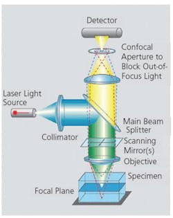
As shown in Figures 1a and 1b, there's a great difference between a conventional microscope and a confocal one. Traditional microscopes focus a magnified area of the specimen to an area of the viewer's eye. A confocal microscope images only a single point at a time rather than an area.
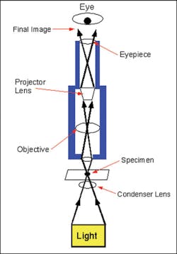
Figure 1a. Conventional Microscope Optical Path
Courtesy of Miami University, College of Arts and Science
In 1988, the editor of Scanning, The Journal of Scanning Microscopies asked Marvin Minsky, the inventor of the confocal microscope, to describe how the invention had come about in 1955. At the time, more than 30 years earlier, Dr. Minsky was pursuing his interests in mathematics and biology as a Junior Fellow at Harvard University. He particularly wanted to learn more about how the brain worked, the theme of his doctoral thesis at Princeton University.
In his 1988 Memoir on Inventing the Confocal Scanning Microscope,• Dr. Minsky described the problem that was frustrating him. Although you could pick out a few neurons and then stain all the fibers that extended from them, this technique allowed only one cell at a time to be visualized. To understand how the brain learns something, you need to develop a wiring diagram that represents how all the cells are interconnected.
And here was a critical obstacle: The tissue of the central nervous system is solidly packed with interwoven parts of cells. Consequently, if you succeed in staining all of them, you simply can t see anything. This is not merely a problem of opacity,• he continued, because if you put enough light in, some will come out. The serious problem is scattering. Unless you can confine each view to a thin enough plane, nothing comes out but a meaningless blur.
As seems typical of many inventions, a simple, elegant solution eventually presented itself. Dr. Minsky wrote, One day, it occurred to me that the way to avoid all that scattered light was to never allow any unnecessary light to enter in the first place.• The arrangement of a beam splitter, a pinhole, and an objective lens shown in Figure 1b forms a focused image of a single point on the specimen at a conjugate plane, the pinhole ensuring that light from only one point is imaged. The term confocal describes this optical configuration.
Either the specimen or the point being focused must be scanned to create a complete 2-D image. Dr. Minsky's original transmission microscope moved the specimen in a pattern that mimicked a TV raster. Modern reflecting confocal instruments, as shown in Figure 1b, use scanning half-silvered mirrors to move the illuminating laser light in a similar pattern. Data representing the intensity of light reflected from each point then is assembled by a computer to form a visible image.
Low-cost lasers and computers have made the confocal microscope commercially practical, but the operating principles are the same as those of the 1955 prototype. For MEMS observation, the most relevant characteristic of the invention is its very small depth of field, which means that an image is formed representing a thin slice through the specimen. The pinhole blocks most of the light from points not in focus. By vertically repositioning the specimen, a series of slices can be acquired and reassembled into a 3-D image.
The Carl Zeiss LSM 5 PASCAL Laser Scanning Microscope is such a confocal microscope. According to the company, The laser beam is made to scan the sample in X and Y directions, point-by-point and line-by-line. As the laser focus travels along the X and Y coordinates, it generates an optical section of the sample. After the sample has been shifted along the optical axis (Z), the laser beam creates another optical section of a different sample plane.
Successive shifting and scanning create a stack of digital images. From this data, software computes intensity projections with extended depth of focus, intensity or height profiles, topographic maps, or surface topographies of the sample. Figure 2 shows the 3-D surface topography of a MEMS microcomb drive developed from 100 separate 604 • 604 pixel sections corresponding to a 115.5 • 115.5 m area and a 26.7- m height.
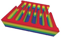
Figure 2. 3-D Image of Microcomb Drive
Courtesy of Carl Zeiss
Interference Fringe Counting
Several related methods are available that divide a beam of light into two beams, insert a variable delay in one of them, and recombine the beams to create a series of interference fringes.
Typically, the spacing of the fringes can be adjusted by changing the angle of the reference mirror used to reflect and delay one of the beams. A larger angle of reflection results in more closely spaced fringes. In practice, one beam reflects from the specimen to be examined and the other beam from the reference mirror. The resulting fringe pattern is a function of the specimen height as well as the reference mirror angle.
An interference image is difficult to interpret for a couple of reasons. First, noncontact interferometry generates symmetrical fringing either side of a zeroth order fringe. Fringes are numbered starting with the one caused by interference of light beams most nearly having the same phase. A fringe occurs every one-half wavelength, so the first, second, third, and higher order fringes will appear periodically on both sides of the central, zeroth order fringe.
If you know the wavelength of the light being used, you can measure height by counting fringes. In addition, if white light is used, by noting the progression of the spectrum of interference fringe colors you can determine whether the specimen surface is rising or falling in the area being viewed.
Software can help solve the ordering problem as well as interpolate between fringes. Nevertheless, interference microscopy is best suited to measuring small height differences within a limited range. For example, in a paper published in the Proceedings of the Society of Photo-Optical Instrumentation Engineers (SPIE), the authors comment that using infrared light (IR) with wavelengths between 8 to 12 m, surface roughness on the order of 100 m could be measured.
White light, originally used in scanning white light interferometry (SWLI), produced too much noise when the light reflected from rough surfaces. Changing to IR reduced this effect. Interestingly, the authors specifically commented about the IR source. Our IR scanning technique also relies on a broad spectral bandwidth to remove fringe order uncertainty, using a glowing filament as the light source. 1
Some interference microscopes may include a means of vertically scanning the light source. This technique measures the phase change occurring in the fringe pattern for each height increment. Ambios Technology calls this type of phase measurement Smooth Mode in the company's Xi-100 Non-Contact Optical Profiler. Step heights larger than one-quarter wavelength can confuse phase measurements made with monochromatic light, so the company recommends this mode be used to obtain high-resolution images of very smooth surfaces.
Ambios provides a Texture mode that uses white light to extend the measurement range to about 100 m. Camera images are stored as a series of frames corresponding to a range of height increments. The company's Xi-100 software reassembles the slices and displays the resulting images.
In the PhotoMap 3-D profilometer from Fogale nanotech, white-light interferometry is used together with very accurate Z-axis displacement to provide 0.1-nm height resolution over a 500- m range. As in the Ambios product, horizontal slices are imaged at successive heights. In addition to creating various surface displays, the Fogale nanotech software also stitches image areas together to cover much larger sample sizes. Micro Photonics is the U.S.A. agent for Fogale nanotech.
Observing MEMS in Motion
Laser vibrometry is the principle behind many Polytec instruments. For example, in the company's model MSA-400 Micro System Analyzer, Doppler vibrometry measures vibrations along the axis of the microscope optics (out-of-plane), and stroboscopic video microscopy handles displacements orthogonal to the optical axis (in-plane). The in- or out-of-plane nomenclature refers to a plane parallel to the surface of the MEMS device being studied.
Doppler vibrometry is based on the modulation of interference fringes caused by specimen motion. Rather than a stationary fringe pattern, which constructive and destructive interference produces in an interference microscope, the pattern in a Doppler vibrometer is moving at a rate proportional to the MEMS device motion. By measuring the time rate of change in distance between successive fringes, a vibrometer can determine how fast a MEMS device is vibrating.
Similar to the fringe ordering problem associated with interference microscopes using monochromatic light, the laser interference fringes measured by a vibrometer cannot distinguish the direction of MEMS motion. Polytec solved this problem by inserting a Bragg cell in the reference arm of the optical path, causing a 40-MHz offset to the laser frequency. This means that a 40-MHz modulation exists when the MEMS device is at rest.
As a result, the direction of motion can be determined by observing the Doppler effect on the modulation frequency when the MEMS device is operating. The frequency reduces as the device moves toward the vibrometer and increases when it moves away from the instrument. The amount of the increase or decrease depends on the speed of motion.
In principle, because a vibrometer is presented with several fringes just as is an interference microscope, displacement can be measured as well as velocity. Displacement demodulation is better suited for low-frequency measurements and velocity demodulation is better for higher frequencies because the maximum amplitudes of harmonic vibrations can be expressed as:
v = 2πfswhere: v = velocity
f = frequency
s = vibration amplitude
As frequency increases, a certain vibration generates higher velocities at lower displacement amplitudes. 2
Scanning the laser beam over an area of the device being examined will develop a 2-D image. Different vibration modes simultaneously occurring, such as resonances on separate parts of a structure, can be shown. However, Doppler vibrometry primarily measures out-of-plane vibration, and in-plane motion is detected via coupling to an out-of-plane mode.
Holographic interferometry and electronic speckle pattern interferometry are similar. Both techniques record so-called speckle patterns formed by the interference among light rays reflected from a vibrating surface. If two speckle patterns obtained at slightly different times are subtracted from each other, a correlation fringe pattern is obtained that corresponds to the vibration amplitude.
Optonor's MicroMap 5010 is a miniature TV-holography system. It performs both static displacement and vibration measurements but cannot be used for fast transients because time averaging is required on steady-state vibration modes. According to the company, the MicroMap 5010 can measure both rough and smooth surfaces down to an area of 245 • 330 m with spatial resolution to 3 m. Vibration frequencies up to 20 MHz are handled by the standard system, but measurements to 500 MHz or greater are possible.
To capture in-plane motion, stroboscopic techniques can be used. Most people are familiar with the apparent precession of wagon wheel spokes in western movies. The frame rate of the cinematic camera causes this stroboscopic effect by accidentally synchronizing to the speed of the wagon wheel. At a certain wagon speed, the positions of the spokes on successive frames are nearly identical. The same effect can be produced by flashing a light to synchronously illuminate a moving object.
In Polytec instruments, a pulsed LED is used as the stroboscope light source, the system's time resolution being determined by the width of the strobe pulse. By adjusting the repetition rate of the light pulse, in-plane motion can be frozen and examined. Polytec advises that short strobe pulses are necessary to freeze a rapidly moving structure. Blur is generated if the device moves a longer distance than the distance corresponding to the diameter of one camera pixel during the strobe illumination.3
Electrical Testing
Frequencies associated with MEMS devices generally are low enough that conventional electronic instruments are suitable. For analyzing waveforms corresponding to complex mechanical motion, a dynamic signal analyzer is a good choice. Very high-frequency oscillators may require a network analyzer for full characterization. And, to provide complex drive waveforms, an arbitrary signal generator can be useful. Otherwise, general-purpose scopes, power supplies, and signal generators and amplifiers work well.
Storrs Hoen, a project manager in Agilent Technologies• Life Science and Nanotechnology Department, described some of the MEMS test instrumentation used in his work. An Agilent Infiniium scope sits adjacent to our test board, allowing us to test signal integrity, perform FFTs to look for noise sources, and verify device timing.
To characterize capacitive sensors, we use a Model 89410 Vector Signal Analyzer. Its white-noise source allows us to determine the best operating frequency for our synchronous drive,• he explained, and its calibrated noise floor provides a key check of our circuit models. A dynamic signal analyzer is used for mechanical analysis. The analyzer's low-frequency swept sine capability precisely determines a device's modal response. Also, we have used Series 8700 Network Analyzers to determine the frequency response of film bulk acoustic resonators (FBAR) and MEMS frequency standards.
FOR MORE INFORMATION Agilent TechnologiesModel 35670A Dynamic Signal Analyzer www.rsleads.com/609ee-176Ambios TechnologyXi-100 Noncontact Optical Profiler www.rsleads.com/609ee-177Carl ZeissLSM 5 PASCAL Laser Scanning Microscope www.rsleads.com/609ee-178Micro PhotonicsFogale nanotech Photomap 3-D Profilometer www.rsleads.com/609ee-180OptonorMicroMap 5010 www.rsleads.com/609ee-181PolytecMSA-400 Micro System Analyzer www.rsleads.com/609ee-182TEGAM Model 9070 MEMS Engine Driver System www.rsleads.com/609ee-183Tokyo ElectronTEMEON MEMS Tester www.rsleads.com/609ee-184TEGAM stresses the fidelity of the company's MEMS test equipment, and this is a valid point. It's no good being able to provide a 200-V pulse signal if it rings or is distorted. Although test equipment with good performance is available from several vendors, TEGAM offers a group of instruments as a MEMS testing solution. When dealing with other manufacturers, you may need to assemble such a test capability yourself from various catalog entries.
Adam Fleder, TEGAM's president, described a MEMS micro-mirror testing example. An optical interferometer is used in the testing of adaptive optic systems utilizing MEMS mirrors. Precise wideband control of the mirror drive signals and synchronization of the optical sensing system are accomplished by a selection of TEGAM instruments. Our amplifiers• slew rate and stability avoid overshoot in the actuator drive signal that would cause the MEMS mirror to deflect beyond its design point or require a delay while it settled.
The testing of RF MEMS devices also poses unique challenges,• he continued. A specially shaped actuation pulse must be generated and synchronized with a network analyzer to coordinate the MEMS switch RF parameter characterization in both the closed and open states.
MEMS Production Testing
In addition to instruments that can measure electrical and mechanical parameters, testing MEMS devices requires various types of stimuli. Some MEMS transducers are sensitive to vibration, others to acceleration or rate of rotation, and still others to pressure. The characteristics of most MEMS devices change over the full range of operating temperatures.
To address these issues, Tokyo Electron (TEL) has developed the TEMEON product specifically for wafer-level MEMS testing. As Masami Yakabe of the TEL-MEMS department in Tokyo explained, The TEMEON tester applies a unique local vibration stimulus that activates mechanical movement while the instrument also measures the electrical signals. TEMEON uses new contact technology that enables much more accurate measurement results because only one-tenth of the contact force normally required is needed to achieve a low contact resistance.
This ultra-low contact force is important because MEMS devices are sensitive to outside pressure. For example,• he continued, accelerometer testing on TEMEON is achieved at the wafer level. This allows MEMS devices to be tested and the characteristics measured accurately before dicing and packaging. The TEMEON measurement specification includes a sufficiently high signal-to-noise ratio to measure the minute signals generated by today's MEMS devices.
At the packaged part level, the FocusTest MPX-2 ATE System addresses both mechanical and electrical test requirements across multiple DUTs. A custom multisite test fixture interfaces to the appropriate mechanical stimulus, depending on the nature of the MEMS device being tested. The system includes power supplies, a five-slot FocusTest instrument chassis, a PXI instrument chassis, and test software based on National Instruments TestStand and LabWindows/CVI.
The company's Brian Colozzi emphasized the capability of the Focus-Test instruments and Smart-Connect• Loadboard to support eight MEMS devices. Each DUT is provided a separate controller, four drive/compare digital pins, and an additional eight digital I/O pins. Each channel has its own 512-kB memory for DUT setups, special coordinated measure routines, and DUT output acquisition storage for post-test analysis.
Summary
MEMS devices present special test challenges. For example, handling and contacting methods similar to those used with purely electrical ICs may not be appropriate. Because of a device's mechanical properties, operation can be distorted by externally applied forces. This consideration led to development of TEL's TEMEON wafer-level test system and to the special test fixtures associated with the FocusTest MPX-2 Test System.
It's particularly important that the mechanical test stimulus is applied in such a manner that the MEMS device operates as it would in its intended application. When that has been verified, readings from your chosen noncontact profilometer or electrical test instruments will be relevant.
References
1. de Groot, P., et al, Step Height Measurements Using a Combination of a Laser Displacement Gage and a Broadband Interferometric Surface Profiler,• Proceedings of SPIE, Vol. 4778, 2002.
2. Measurement Solutions Made Possible by Laser Vibrometry, http://www.polytec.com/usa/_images/LM_AN_INFO_0103_E_Vibrometry_Basics.pdf
3. 3-D Vibration and Motion Analysis of Microstructures,• INFO, Polytec Newsletter, Issue 1/2005.
About the Author
Comment About the Article
To join the conversation, and become an exclusive member of Electronic Design, create an account today!

Leaders relevant to this article: