Testing Challenges of a Multicore Microprocessor
The Cell Broadband Engine is an advanced multicore microprocessor optimized for compute-intensive workloads and various broadband media applications including computer entertainment, movies, and other forms of digital content. Testing the performance of this high-volume processor is challenging. To appreciate the magnitude of this task, let's start with an overview of the design-for-test (DFT) aspects of the Cell processor and its demands on the automatic test pattern generation (ATPG) products used to produce tests for it.
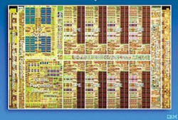
Cell is a heterogeneous chip multiprocessor that consists of an IBM• 64-b PowerPC Architecture• core (PPE) and uses high-frequency clocks that can run near 4 GHz. It is augmented with eight specialized co-processors based on a single-instruction multiple-data (SIMD) architecture called the Synergistic Processor Element (SPE), which addresses data-intensive processing like that found in cryptography, media, and scientific applications. The system is integrated by a coherent 128-b on-chip bus (Figure 1).

Based on the analysis of available die area, cost, and power budgets, the best approach to achieving the performance target was to exploit parallelism through a high number of nodes on a single-chip multiprocessor. To further reduce power, the team opted for a heterogeneous configuration that combines the flexibility of a PowerPC Architecture core with the functionality and performance-optimized SPE SIMD cores.1,2
Testing the Cell Processor
A key requirement for the Cell design was a low pin-count test strategy. To achieve this objective, the functional and test pins are shared. When in the test mode, 64 pins are designated as scan pins. The default test configuration for these 64 pins is defined as 32 scan-ins and 32 scan-outs.
Alternately, the 64 pins can be defined as 64 scan-in or 64 scan-out pins. An additional 34 pins are used for test control. Another 32 pins are used for I/O testing and reference clock inputs. The total number of test pins required is 128. This low pin-count enables the use of low-cost testers and multidevice testing.
From a modularity perspective, the Cell test logic is structured to allow different combinations of PPE and SPEs to exist on a chip. From a test perspective, this capability requires a pervasive logic design to manage different numbers of processor cores efficiently.
Built-in self-test (BIST) engines are designed to reside in a stand-alone or satellite mode. A flexible infrastructure supports varying numbers of BIST engines. To address core redundancy, additional logic has been added to the test infrastructure to assist with testing individual core components.
Each device that resides on the Element Interconnect Bus (EIB) can be isolated and tested in the stand-alone mode. Also, the scan structure and isolation mechanism prevent the cores from contaminating each other and allow for quick diagnostics of a core when a defect is detected.
Test Generation Challenges
The Cell processor is a high-speed design with a highly pipelined data flow. To increase performance, reduce power consumption, and conserve real estate, a trade-off was made so that most of the data-flow pipeline stages would not be scanned.
To avoid making the design too deep for ATPG to process in a reasonable amount of time, only three consecutive stages of data-flow pipeline were permitted in the design. This meant that even static ATPG would require at least four clock cycles per test: three to get through the non-scan pipeline plus one more to capture into a scan element. In the final design, the Cell processor's first implementation has about 40% non-scan flops.
Pipelines also are required to stop the processor synchronously. In a high-speed design of this nature, it is not possible to reach all storage elements in a single processor clock cycle. Consequently, the stop signal must be pipelined to all storage elements through equal-depth, free-running pipelines. Once the chip is stopped, slow-speed signals can be propagated around the chip for reconfiguration purposes, at which point the stop can be synchronously removed.
Several aspects of the Cell processor design made it a bit more difficult than usual to generate tests. Most of the DFT aspects of this design would be considered normal support for any ATPG and Logic BIST (LBIST) tool set, including support for some non-scan pipelines in the data flows of the design. However, pipelining scan-enable and other control signals created an additional challenge for the EDA tools.
Since the control signal pipelines in the Cell processor are more than 25 stages deep, going back 25+ clock cycles takes you within the scan load operation. In addition, some of these control signals must switch at the end points of the pipelines just as the scan operations are ending, implying that the pipeline input has to switch 25+ cycles before the end of the scan.
And that is just the beginning. Other control signal changes within the tests have to migrate back 25+ clock cycles into various points within the last few scan cycles.
Test Modes
The Cell test design focused on using a reduced number of pins. To achieve this objective, several test modes were incorporated into the design to allow for pin reuse. Test pins are shared with functional pins.
Full Access Mode
For Full Access mode, the scan chain structure connects all of the scan latch elements so the entire chip can be scanned at once. This mode uses 32 scan inputs and 32 scan outputs.
Full Access mode can be used to initialize other modes, such as LBIST, and run ATPG patterns. This mode provides the capability to initialize the chip to any desired state.
In Full Access mode, both the Cell core logic and I/O blocks can be scanned. Thirty scan-in pins are dedicated to the core logic and two scan-in pins to the I/O blocks. Likewise, 30 scan-out pins are assigned to the core logic and two scan-out pins to the I/O blocks.
Memory BIST
Cell uses a scan-access memory BIST approach. But true at-speed testing requires at least two accesses on successive grid clock cycles. This requirement is met by providing shadow flip-flops (FFs) in the scan path before each RAM address bit and control bit FF along with just one shadow data FF for the full RAM data register.
The chip is held in the scan mode during the execution of memory BIST. Once the values for the first access are set, the values for the second access are set on the very next clock pulse.
Access cycles are controlled by a trigger signal that is sent in parallel with the access values. Staging FFs can be added to both value and trigger on the path to the RAM and on the path back to bridge the distance. Here again, scan-at-ship-speed is needed to support back-to-back memory accesses. Also, scan-at-ship-speed optimizes tester time for a scan-style memory BIST.
Logic BIST
The Cell chip uses a programmable LBIST controller instantiated in the Test Control Unit. The LBIST configuration adheres to a general self-test using a multiple input signature register and parallel shift register sequence generator (STUMPS) architecture for the scan chains.3
Scanning in Full Access mode allows the controller to be initialized for many predefined clocking sequences that launch and capture data within the data pipelines. The controller can operate at system design speed with on-product clock generation (OPCG) or with up to 200-MHz ATE clocks.
To distribute the scan/control signals across the chip area, specific implementation pipeline flops are used to stage the requests to scan or capture data. To prevent excessive power during scanning, the controller can be programmed to scan from one-half to one-eighth the rate of the system clock in OPCG mode. The LBIST sequences also can be applied directly from chip inputs.
Compressed Deterministic Tests With OPMISR+
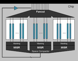
For deterministic tests, on-product multiple input signature register (OPMISR+) compression is used on the Cell processor.4 OPMISR+ mode configures the 32 scan-in pins and 32 scan-out pins as 64 scan input pins.
Careful mapping of the scan channels maximizes efficiency. For example, all SPEs are loaded from the same scan inputs. This approach allows all eight SPEs to be scanned simultaneously with the same data.
Scanning efficiency is far improved over Full Access mode. For example, scanning an SPE in OPMISR+ mode takes approximately one-twelfth the time that would be required in Full Access mode, a result of scanning into 24 scan channels vs. two.
OPMISR+ compression also supports masking logic.5 Loading of the masks occurs prior to scan unloading. But for Cell, there is no support for switching between scan loading of masks and normal scan if both use the grid clock. Mask loading must be done using a different clock.
The mask-enable signals are treated as a scan input from the ATE perspective. An example of OPMISR+ configuration with masking is shown in Figure 2. Since the Cell processor is designed to be X-free for LBIST, it does not include any masking logic in its current implementation.
I/O Test Mode
The I/O test mode configures the Cell processor to enable the dedicated test interface for the high-speed I/O units. In this mode, the tester can scan and run ATPG on I/O block units. When I/O test patterns are being executed, the core Cell logic provides fixed values to the boundary of the I/O units.
Functional Scan Mode
While in Functional Scan mode, there are two base scan configurations available. The standard configuration connects the scan latches of a unit into one scan chain. For example, an SPE will be configured so that all flops in that unit are connected into one scan chain. The alternative mode provides a long scan chain that contains all scan latches of all units on the chip.
The I/O blocks are not included in the long scan chain but are available in the standard configuration. The IEEE 1149.1 (JTAG) interface accesses these chains. These scan chains are used for lab bring-up and debug.
The Test Control Unit has a JTAG controller that can access the majority of the scan latches. Also, special commands have been created to allow tests to be started and stopped. This capability allows the automatic BIST (ABIST) and LBIST manufacturing sequences to be debugged on lab bring-up.
Verification Mode
Advanced Verification Program (AVP) mode provides a mechanism to allow programs to be run on a manufacturing tester. In this mode, the internal arrays of the processor can be loaded with a program and executed. This mode does not require data on the scan-in and scan-out pins.
AVP mode only provides a mechanism to run a program. Scanning data into arrays for use by AVP mode is done in Full Access mode or OPMISR+. AVPs are functional programs that can measure power and frequency limitations while a functional test case is running on the manufacturing tester.
Partially Good Die
To help improve the yields on many complex chips with embedded RAM, redundancy allows for some defects to be bypassed and still ship a functioning chip to customers. While RAM redundancy is quite common, logic redundancy is rare.
The Cell processor implements a form of logic redundancy that allows for up to one defective SPE core. The defective SPE can be fully disabled, and the Cell processor simply will use the seven available SPEs for scheduling the tasks assigned for execution on SPEs. To ensure consistent execution times, customers can force one SPE to be disabled even with an all-good chip.
Much thought went into the DFT for the Cell processor, especially regarding how to deal with allowance for partially good devices. Each SPE core is effectively isolated during most of the testing, and if errors appear on scan chains from a specific SPE, that SPE is noted as being defective. Errors detected outside of an SPE or from multiple SPEs will cause the whole chip to be considered defective.
Results
The test modes and test sequences developed for the Cell design have worked well for test-pattern development and pattern debug. Use of partially good die has helped improve yields for this high-volume device.
References
1. Kahle, J.A., et al., Introduction to the Cell Multiprocessor,• IBM Journal of Research and Development, Vol. 49, No. 4/5, 2005.
2. Riley, M., Bushard, L., Chelstrom, N., Kiryu, N., and Ferguson, S., Testability Features of the First-Generation Cell Processor,• Proceedings International Test Conference, 2005.
3. Bardell, P.H. and McAnney, W.H., Self-Testing of Multi-Chip Logic Modules,• Proceedings International Test Conference, 1982, pp. 200-204.
4. Barnhart, C., et al., Extending OPMISR Beyond 10X Scan Test Efficiency,• IEEE Design & Test of Computers, September-October 2002.
5. Chickermane, V., Foutz, B., and Keller, B., Channel Masking Synthesis for Efficient On-Chip Test Compression,• Proceedings International Test Conference, 2004, pp. 452-461.
About the Authors
Louis Bushard, Ph.D., is a senior engineer, custom DFT at IBM. Before joining the company in 1996, Dr. Bushard was a mathematical programmer for Babcock & Wilcox and a logic designer at Cray Research, Sperry Rand Univac/Unisys, and Star Technologies. He graduated with a degree in mathematics from the University of Minnesota and completed a post-doctoral research fellowship at Wright-Patterson Air Force Base. IBM, Mail Drop: HPK, Building 040, Floor 3, Office B414, 605 Hwy. 52 N, Rochester, MN 55901-1407, 507-253-6216, e-mail: [email protected]
Nathan Chelstrom is involved in DFT at Intrinsity. Previously, he was in logic and test architecture at IBM and logic and DFT at Motorola. Mr. Chelstrom has authored two ITC papers regarding the Cell processor and testability/debug features and was an ITC 2005 panel speaker addressing test challenges for SOCs and multicore designs. Intrinsity, 11612 Bee Caves Rd., Building II, Suite 200, Austin, TX 78738, 512-421-2241, e-mail: [email protected]
Steven Ferguson is the STI DFT team leader at IBM in Texas. He joined IBM in Tucson in 1978 after six years in the U.S. Army. Mr. Ferguson has held positions in manufacturing test engineering and ASIC and custom engineering since 2003. IBM, 11501 Burnet Rd., Austin, TX 78758, 512-838-7257, e-mail: [email protected]
Brion Keller is a senior architect for the Encounter Test R&D Team at Cadence Design Systems. He obtained a B.S. in computer science and chemical engineering at Penn State University. Mr. Keller has been pursuing interests in ATPG, fault modeling and simulation, logic BIST, and compression for more than 27 years and is an inventor on seven issued patents and several pending ones. Cadence Design Systems, 1701 North St., Endicott, NY 13760, 607-762-1347, e-mail: [email protected]
About the Author
Comment About the Article
To join the conversation, and become an exclusive member of Electronic Design, create an account today!

Leaders relevant to this article: