Helping Signals Retain Their Individuality
Signal integrity (SI) issues include any effects that distort a signal. Early telephone systems and transatlantic cables had SI problems long before microprocessors and digital communications proliferated.
The term applies to all signals, both analog and digital, but has become closely associated with high-speed digital signal quality through familiar displays such as eye diagrams and bathtub curves. By considering amplitude and timing separately, the problem can be simplified, although assigning a specific cause to either effect can be difficult if you are working only with the corrupted signal.
In a presentation made to Lockheed engineers in 2000, Dr. Eric Bogatin listed more than 20 SI causes and effects, including terminations, emissions, attenuation, ground bounce, ringing, RC delay, IR drop, parasitics, capacitance, and stubs. From the group, he distilled four high-speed problems: impedance discontinuities that cause reflections and distortions, crosstalk, rail collapse, and EMI.
The increase in circuit speed that occurred during the 12 years since the Lockheed presentation has only made correct treatment of SI causes more important. At the time, Dr. Bogatin proposed six design techniques to maintain high-speed signal integrity:1
- Slow down edges.
- Minimize the length of all interconnects.
- Use contolled impedance lines and terminate.
- Use continuous, closely spaced adjacent power and ground planes.
- Use low dielectric-constant material for signal layers.
- Minimize loop mutual inductances between signal lines.1
If a signal’s rise and fall times are significantly slower than the propagation delay through the circuit, reflections will be minimized. Also, slower edge speed reduces high-frequency crosstalk. Inserting series resistors is a simple edge-speed reduction approach that uses a circuit’s stray capacitance to advantage.
When rise and fall times are comparable to or faster than the circuit propagation delay, controlled impedance lines become necessary. Parallel termination works well to eliminate reflections for point-to-point signals. In contrast, series-terminated lines achieve the full signal amplitude at the receiving end only because of reflection. Interconnects can be particularly unfriendly to fast signal edges if the high frequencies see a significant impedance discontinuity.
High capacitance between a PCB’s power and ground planes is desirable because it creates a distributed return path for high frequencies. This can be achieved by using a thin piece of high dielectric constant material between the planes—power-plane to ground-plane capacitance is higher in an eight-layer PCB than in a four-layer one, assuming equal overall thicknesses. Aspects associated with power distribution in high-speed or high-power circuits are called power integrity (PI).
For high-speed signals, an Altera design guide suggested, “To reduce crosstalk in dual-stripline layouts, which have two signal layers next to each other, route all traces perpendicular, increase the distance between the two signal layers, and minimize the distance between the signal layer and the adjacent reference plane.”2
Clearly, the design of a high-performance six- or eight-layer PCB involves many cross-discipline considerations not required in slower applications with fewer, less optimized layers. Typically, systems requiring such PCBs add even further constraints. For example, high-speed digital signals often have added pre-emphasis to increase the amplitude of 0-to-1 or 1-to-0 transitions. Increasing the amount of high-frequency energy mitigates some of the loss suffered as the signal propagates through a medium. But the process also increases the EMI the circuit is capable of radiating.
Design
Especially with the very high circuit density on today’s PCB assemblies and the use of BGA devices that prevent direct access to connections, SI must be addressed at design. ANSYS, MathWorks, and others provide simulation software that handles a design’s thermal, electrical, and mechanical features.
A hypothetical example provided by ANSYS demonstrates the types of conflicts that can arise during a laptop computer design. The SI/PI team might design a PCB that ensures the fidelity of a high-speed link, but two high-power devices have been placed near each other. Attempting to increase the copper area available for heat dissipation could interfere with the high-speed channel layout.
EMC/EMI engineers might want to reduce the size of the air vent to reduce emissions. Of course, thermally, that may not be practical. Alternatively, adding a heatsink increases weight, and a fan reduces overall reliability. To account for all the interactions among the various design elements, ANSYS recommended using a single, integrated simulation program.3
Samtec has concentrated on the SI effects of connectors in high-performance systems and provides electrical models compatible with a range of EDA tools including Advanced Design System (ADS) from Agilent Technologies, Allegro® PCB SI from Cadence, HyperLynx from Mentor Graphics, HSPICE® from Synopsys, ICX® from Mentor Graphics, and OrCAD® Capture from Cadence.
Because several circuit traces are concentrated in a small space, connectors often have a large effect on the surrounding PCB layout. How traces within the breakout region are treated is critical to SI. According to Samtec, “Single-ended traces are referenced to an adjacent ground layer…. Differential traces may be designed as standalone, tightly coupled pair groups, or… as two single-ended traces…. To minimize crosstalk, it is almost always desirable to minimize coupling between signal conductors. Therefore, multiple single-ended traces are spread out as widely as possible. It also is desirable to couple differential pair mates as tightly as possible while at the same time separating each pair from other pairs.”4
A major problem that arises during simulation relates to the validity of the connector model. Of course, any model must truly represent a component’s behavior, but connectors present obvious disruptions to PCB traces and often are physically large.
Because the treatment of the attached traces affects overall performance, how useful is a model of the connector alone? Samtec has created a series of reference designs the company calls Final Inch® for which it provides Gerber files and validated SPICE models. The models include the connector as well as traces in the breakout area and support more realistic and accurate PCB simulations.
Testing
Overview
With so many effects possible, verification by thorough testing is the only way to be certain there are no lurking problems. For data links, bit error rate testing (BERT) compares transmitted and received data, keeping track of the errors. A BERT instrument varies the timing of the receive data sampling point. In this way, a 2-D eye diagram is created relating signal amplitude to time.
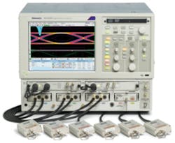
Courtesy of Tektronix
Anritsu recently launched the Model MP1800A Signal Quality Analyzer BERT for data link characterization to 32 Gb/s. Up to 12 pulse-pattern generators can be synchronized within a single mainframe, useful for evaluating multichannel crosstalk. A jitter modulation source is included to support jitter tolerance testing. Bathtub curves and eye diagrams are among the graphical displays available.
A sampling scope or real-time scope also can develop an eye diagram, but these instruments generally take longer to do so and may not provide as much insight about the kinds of errors that occurred. For example, a BERT may compare strings of bits so that you know whether an error occurred on a 0-to-1 transition following three successive 0s or only when one 0 was involved.
A number of displays have been developed to highlight error behavior. The bathtub curve is a plot of timing jitter vs. bit error rate. If a circuit is operating at 1 Gb/s and at a certain error rate exhibits 470 ps of jitter—the sum of the falling and rising edge jitters—the timing margin is 530 ns: the difference between the 1-ns unit interval (UI) and the total peak-to-peak jitter.
Timing
Oscilloscopes are the favorite instrument for investigating timing-related SI issues although not the only one. Regardless of the intricacies associated with a modern, fast DSO’s acquisition and display functions, scopes remain visual instruments. They present pictures of waveforms and signal relationships that, to the trained eye, help to explain SI problems. Nevertheless, just as most high-performance scopes have an FFT capability and can display frequency domain information, many scopes also measure jitter, present eye diagrams, and develop histograms of user-selectable measurement criteria.
Chris Loberg, senior technical marketing manager for performance oscilloscopes at Tektronix, emphasized the need for better measurement accuracy because of the very small margins in today’s high-speed designs: “We were asked to help Intel develop and evaluate a new generation of 20-Gb/s Infiniband optical cables for scaling out advanced computer clusters to distances of up to 100 m. Tek, working with Intel, utilized an AWG7000 Arb to provide a stressed, 5-Gb/s pattern to drive the long cables and a DSA8200 Series Sampling Scope and an 80E10 TDR Module to observe the waveform at the far end.” Loberg said that the combination of test equipment, analysis software, and test technique confirmed the cable’s 10-15 BER specification.
Jitter measurements on a scope are made edge-to-edge within a many-transition acquisition and, in this way, avoid trigger jitter uncertainties. Nevertheless, clock period jitter or data pulse width jitter is not the same as jitter determined by measuring the position of a data edge relative to a reference. This is the type of measurement that a timing interval analyzer (TIA) makes.
Typically, a TIA cannot measure parameters in contiguous UIs in real time—an amount of dead time occurs between each measurement. For example, GuideTech’s Model GT668PCI-2 has 2-ps resolution and accepts signals up to 2.7 GHz but has a maximum measurement rate of 3.5 M-measurements/s. This means that a TIA must have a source of repetitive data if effects such as intersymbol interference (ISI) are to be investigated in very fast data links. TIAs can distinguish among the various types of jitter and may present a variety of SI displays.
GuideTech’s continuous time-interval analyzers (CTIA) timestamp each occurrence of a user-defined event relative to a unique starting point. Total jitter is the variation in the differences between successive timestamps.
Each channel of the Gigamax Technologies (formerly Wavecrest) SIA-4000 Signal Integrity Analysis Solution has an integrated 15-GHz bandwidth sampling scope. In addition, a very stable reference clock supports a range of jitter measurements including random, deterministic, ISI, BER, periodic, pulse width, and rms jitter over a selectable bandwidth. The instrument typically contributes only 200-fs rms of its own jitter from 12 kHz to 20 MHz.
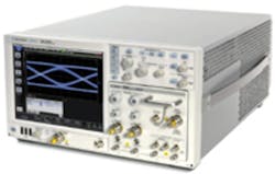
Courtesy of Agilent Technologies
S-Parameters
Another way to characterize a circuit or device is to treat it as a two-port network and measure its S-parameters. Traditionally, this is done using a vector network analyzer (VNA). This instrument sources a clean, narrowband signal with a known phase. The set of four S-parameters comprises the complex ratios of the reflected and transmitted signals with respect to the incident signal.
S-parameters are useful in high-frequency linear design because they are readily available for common devices and can be cascaded. Also, each parameter has a well-understood meaning so anomalies in one or more give clues to SI problems.
For example, S21 is the forward network gain and S22 the output port reflection coefficient. The output voltage is equal to the input signal multiplied by the gain. However, there may be a contribution from the S22 term if the network termination allows significant signal reflection. Similarly, S11 is the input port reflection coefficient and S12 the reverse gain. The input return loss is directly related to S11, the amount of signal that does not contribute to the output because it is reflected at the input.
S-parameter plots pick up problems such as resonances that may otherwise be difficult to observe. According to Dr. Alan Blankman, product manager signal integrity at LeCroy, “Today’s world of high-speed designs has led to an explosion in the use of S-parameters to both model and characterize the passive structures such as backplanes and interconnects used in high-speed serial designs. S-parameters are used to predict signal integrity issues in high-speed designs. SI engineers create S-parameter models using various modeling tools and then validate the models by making measurements with a network analyzer.”
In addition, S-parameters are used to simulate signal behavior at points in the circuit that cannot be physically probed. Dr. Blankman continued, “VirtualProbe [software] allows users to configure a multiblock model of their system and relocate the measurement point to a position different from where the probe was located. This is accomplished by using S-parameters of system components…. By using the virtual probing capabilities, users can perform eye and jitter analysis of signals as they would appear without the effects of fixtures. They also can perform the analysis by including the effects of a channel for which only an S-parameter model is available; this allows users to predict the potential signal integrity effects of a channel, including ISI and crosstalk and jitter effects.”
Trends
There are many facets to signal integrity, but the continuing development of faster and more complex data protocols has focused attention on speed-related issues. Sampling scopes have been used for decades to view fast waveforms, and recently these instruments have been further refined with an emphasis on jitter and S-parameter measurements.
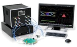
Courtesy of LeCroy
Tek’s Loberg described the changes made to the company’s DSA8300 Series Sampling Scopes to cut the mainframe jitter by 50%, improve vertical resolution to 16 bits, and increase the maximum sampling rate to 300 kS/s. Actual performance depends on the plug-in modules fitted: the 80E09 60-GHz low-noise electrical sampling module or the two-channel 80E10 TDR Module.
According to Tek’s online electrical sampling module information, the 80E10 provides a 12-ps incident and 15-ps reflected rise time. The polarity of the two sources can be independently selected to support differential- or common-mode testing.
Agilent Technologies’ 86100D Mainframe accepts modules with up to 80-GHz bandwidth. The Model 54754A TDR Module, when used with the 86100D, provides a 35-ps rise-time pulse. The edge speed of a TDR pulse is important because it determines the minimum physical length of a discontinuity that can be correctly measured. Agilent cited the equationwhere: e = transmission system dielectric constant; c = speed of light in a vacuum
For a PCB with e approximately 4.5 and c = 3E8 m/s, the distance = 2.4 mm. To improve resolution, the company suggests using a Picosecond Pulse Labs Model 4020 Source Enhance Module, which outputs a 9-ps edge in response to a 35-ps rise-time input. Clearly, the minimum distance reduces in proportion to the change in rise time, becoming 0.6 mm for a 9-ps edge. With the faster edge, the 86118A 80-GHz bandwidth plug-in is recommended.
LeCroy’s SPARQ System provides a 6-ps pulse edge and measures S-parameters to 30 GHz or 40 GHz depending on the model. Systems with up to 12 ports are available. All models feature a single button-press auto-cal based on built-in standards.
References
- Bogatin, E., “Signal Integrity: Problems and Solutions,” 2000.
- Altera Board Design Resource Center, www.altera.com
- “From Signal Integrity to Product Integrity,” ANSYS, White Paper, 2011.
- Interconnect Signal Integrity Handbook, Samtec, 2007, pp. 25, 26.
For More Information
About the Author
Voice Your Opinion!
To join the conversation, and become an exclusive member of Electronic Design, create an account today!

Leaders relevant to this article:


