Software-Designed Instrumentation Redefines Test
Software-based test-system architectures have become increasingly popular over the past several decades. As test applications become more complex, engineers are continuously challenged with the dilemma of increasing functionality without increasing test times and ultimately test cost. While developments in test and measurement algorithms, bus speeds, and CPU speeds have reduced test times, further improvements are necessary to address the continued increase in the complexity of test applications.
One way to minimize hardware costs and reduce test time is to use virtual (software) instruments along with modular I/O; however, a new approach—software-designed instrumentation—uses open user-programmable field-programmable gate arrays (FPGAs) to achieve test time reductions that are orders of magnitude beyond what was previously possible without custom or standard-specific instrumentation.
FPGAs are reprogrammable silicon devices that can be programmed to implement custom functionality. While FPGAs are common in instrumentation, they typically have fixed personalities designed for specific purposes and allow little or no customization. By contrast, open user-programmable FPGAs make it possible for the user to customize instrumentation for specific application needs or to maximize performance.
User-Programmable FPGAs
The RF test space is a prime example of where software-designed instrumentation is needed. The number of wireless devices, diversity of communications standards, and sophistication of modulation schemes are increasing dramatically each year. With each subsequent generation of technology, the cost of testing wireless devices using traditional techniques also increased as a greater amount of more complex test equipment is needed.
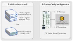
An example of a software-designed instrument is a vector signal transceiver, which combines a vector signal generator (VSG) and vector signal analyzer (VSA) with FPGA-based real-time signal processing and control. The NI PXIe-5644R Vector Signal Transceiver from National Instruments (NI) is the first RF instrument to incorporate this user-programmable FPGA hardware architecture. This software-designed approach gives the vector signal transceiver the flexibility of a software-defined radio with RF instrument-class performance. Figure 1 illustrates the difference between traditional approaches to RF instrumentation and a software-designed approach with a vector signal transceiver.
Figure 1. Traditional Approach vs. Software-Designed Approach for a Vector Signal Transceiver
Although user-programmable FPGAs are widely available for custom board designs and as part of COTS devices, they have not been widely adopted in off-the-shelf instrumentation equipment to date. This is largely because of the specialized knowledge required to program these devices. Programming in hardware description languages generally has a steep learning curve and is restricted to digital design experts.
Higher-level FPGA software development environments, such as the NI LabVIEW FPGA Module, make the latest FPGA technology accessible to a much wider set of engineers and scientists. Using graphical programming, logic can be implemented to define the behavior of an instrument in hardware in much the same way as if the program was running on a PC. In fact, the graphical dataflow nature of NI LabVIEW system design software is well suited for implementing and visualizing the type of parallel operations that can be implemented in digital hardware.
For a software-designed instrument to be immediately usable without first requiring extensive programming by the user, it must be supplied with code that implements common default functionality and is precompiled and ready to run out of the box (Figure 2). This functionality should be similar to what is commonly provided by typical instruments of the same type, such as a VSA or VSG. For example, the NI PXIe-5644R includes a precompiled FPGA bitfile or bitstream along with a host interface or instrument driver, which is familiar to RF test engineers.
Figure 2. Software-Designed Instrument with Defined Out-of-the-Box Functionality for Simplifying the Starting Experience
Open FPGAs
There are many opportunities for software-designed instrumentation to enhance RF test. Data reduction is a prime example where decimation, channelization, averaging, and other algorithms running on the deterministic, parallel FPGA fabric implement high-throughput processing and decision making. This decreases test time by reducing the necessary data throughput and processing burden on the host CPU; it also allows for increased measurement averaging for a higher statistical confidence level.
FPGAs can further reduce test times by communicating directly with a DUT and sequencing tests on the FPGA, with the test instrument and DUT changing states in synchronized steps. Other examples of application-specific FPGA designs include custom triggering, fast Fourier transform engines, noise correction, power measurements, inline filtering, variable delays, and power-level servoing.
Software-designed instruments also can help bridge the gap between design and test, enabling test engineers to incorporate or validate aspects of the design before it is complete and for design engineers to use instrument-class hardware to prototype their algorithms and evaluate designs earlier in the design flow.
Example: FPGA-Based DUT Control and Test Sequencing
In addition to RF input and output, software-designed instruments such as the NI PXIe-5644R Vector Signal Transceiver can include digital I/O directly connected to the user-programmable FPGA. By implementing digital protocols such as I2C, SPI, or other custom protocols on the FPGA, the instrument can directly control the DUT. The FPGA also can perform test sequencing, signaling the DUT to change states and immediately trigger RF performance measurements once the DUT is stable (Figure 3).
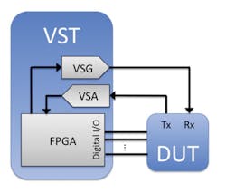
Figure 3. Real-Time DUT Control over Digital I/O
Example: Power-Level Servoing for Power Amplifier Test
In wireless communications systems, a power amplifier (PA) IC is used to increase the signal strength before sending it to the antenna. PAs typically are specified to have a certain performance at a particular output power level, and, therefore, it is important to test them while operating at that output power level. However, the gain of the PA typically is only roughly known and nonlinear over the operating range of the device. The closer the PA is to its maximum output power, the lower the gain.
For these reasons, it is important to level the PA’s output to a known absolute value prior to taking any performance measurements, even outside the linear operating modes. To accurately calibrate a PA, a power-level servo feedback loop is used to determine the final gain. Power-level servoing captures the current output power with an analyzer and controls the generator power level until the desired power is reached.
This can be a time-consuming process, as much as five seconds when using traditional instrumentation, and most of this time is spent controlling the instrumentation through GPIB or Ethernet. Much of the instrument downtime can be eliminated with a vector signal transceiver because the control loop can be implemented directly on the user-programmable FPGA (Figure 4). The result is a much faster convergence to the desired output power value of less than 5 ms.
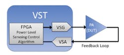
Figure 4. Power-Leveling Servoing
With an open FPGA and flexible hardware architecture, a software-designed vector signal transceiver can go beyond the traditional waveform-based VSA/VSG paradigm. For example, a vector signal transceiver can be redesigned to perform complex, real-time, inline processing for RF applications such as prototyping new RF protocols, implementing software-defined radios, and emulating RF channel impairments.
This software-designed paradigm opens up a world of opportunities for companies with domain expertise to develop FPGA-based intellectual property (IP). National Instruments already has partnered with several companies that can develop and sell IP for the vector signal transceiver, much like companies develop and sell apps for smartphones today. For example, Averna, a National Instruments Platinum Alliance Partner, has developed the vector signal transceiver-powered test instrument—a Data Over Cable Service Interface Specification (DOCSIS) channel emulator.
Averna is a test engineering company with extensive expertise in RF test solutions, including in the broadband equipment industry. For multiple-service operators (MSOs) and certain industry organizations, Averna offers test solutions to ensure that devices such as cable modems, set-top boxes, and residential gateways can provide and maintain a high quality of service. This is particularly important in light of common cable-plant and field interruptions like micro-reflections, phase noise, additive white Gaussian noise, and group delay.
To test their products, MSOs and device makers must simulate numerous real-world conditions with a fully featured cable network, including a cable-modem termination system and whatever customer-premises equipment (CPE) they need to test. Once the test network is simulated, they add the requisite impairments to various channels to test and measure the response of the DUT.
Over three years ago, Averna began developing a standalone desktop channel emulator to address the needs of its broadband customers who wanted to certify their devices to meet the DOCSIS 3.0 standard. At its core, the original DOCSIS channel emulator (DCE) included a mix of off-the-shelf RF hardware instruments and NI FlexRIO modules for signal acquisition, signal impairment, and signal generation for DOCSIS performance testing (Figure 5).
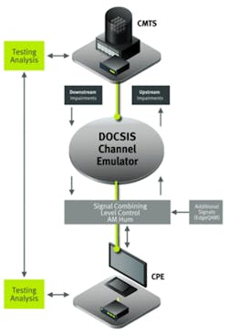
Figure 5. DCE Simulating a Cable Network for Full Device Testing and Measurements
While the original DCE met existing requirements, it became clear during its initial implementations that higher industry channel counts and evolving CPE certification requirements would increase the DCE’s cost, footprint, and system latency while likely making it less adaptable to further changes in the industry. Since the DCE’s raison d’être was to address a wide range of end-user applications by being an inexpensive, flexible, and low-latency instrument, adding increasingly complex hardware was not an option. Therefore, Averna’s developers decided to re-architect their channel emulator with an even greater FPGA focus.
During discussions about its DCE redesign with National Instruments, Averna learned about the NI vector signal transceiver and decided to use it to replace several key components. The vector signal transceiver’s software-designed FPGA approach mirrored Averna’s desire to handle the bulk of its processing and impairments with software rather than hardware. By replacing the physical RF signal analyzer and RF signal generator, Averna also could leave room for future channel-emulation applications. That way, if there were new customer requirements or changing industry specifications, Averna could simply reprogram rather than retool.
After implementing the vector signal transceiver, Averna added some of its own software to collect a broadband signal and extract up to eight individual channels, which it combined to create eight parallel channel emulators. Then the company wrote custom software to stitch the eight channels back together. This allows a single NI vector signal transceiver/NI FlexRIO pair to replace eight transmitter/receiver pairs that otherwise would need specialized and expensive hardware instruments for each channel. To further underscore the need for such a flexible approach, the DOCSIS industry is moving toward chips that support 24 (and possibly 32) bonded channels, making a hardware-based test system an extremely unwieldy and expensive proposition.
To equip the DCE with the signal impairments necessary for DOCSIS compliance testing, Averna assembled numerous channel blocks (or algorithms) from LabVIEW FPGA code and VHDL from Averna, NI, and various third parties. Averna then used LabVIEW system design software to glue all of these blocks together, optimizing them to make the best use of the FPGA resources, which provided not only hardware integration, but also a way to link different modules into a single platform. This expandable library of impairments includes phase noise, micro-reflections, burst noise, frequency shift, carrier-to-noise ratio, composite triple beat, and carrier-to-interference ratio.
During runtime, two FPGAs are used to create the impairments: one on the NI vector signal transceiver and one on the NI FlexRIO. This capability is a significant improvement over the previous-generation DCE. To seriously reduce system latency, the current DCE offloads algorithms that are not in the main data path to the NI FlexRIO. For example, to apply phase-noise impairments, the DCE generates a phase-noise profile that it applies to the signal using complex multiplication. The multiplication needs to be in the main data path so it is performed on the vector signal transceiver whereas the phase-noise profile is generated on the NI FlexRIO to optimize throughput.
Finally, courtesy of its new software-based architecture, the desktop DCE test system has a maximum amount of functionality and flexibility supported by a minimum amount of robust and easily programmable hardware. By combining the functionality of an RF signal analyzer and RF signal generator plus an NI FlexRIO module, the DCE’s current architecture ensures it has a small footprint, greater application flexibility, wider net bandwidth, lower latency, and a lower price point than its earlier incarnation, as shown in Table 1.
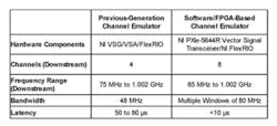
Table 1. Previous-Generation Channel Emulator vs. Software-Designed DCE Feature and Performance Benefits
Multiple Possibilities
Open, FPGA-based RF instrumentation, such as a vector signal transceiver, represents a new class of instrument that is software designed with the capability to adapt hardware functionality to application requirements. As RF devices become more complex and time-to-market requirements become more challenging, this level of instrument customization gives control back to the RF designer and test engineer. These examples represent a small sample of possible user- or application-specific enhancements.
About the Authors
Erik Johnson, the product manager for RF and wireless test at National Instruments, has spent nearly seven years in the test & measurement industry. During that time, he has served in a variety of roles, including applications engineering, field sales, and RF systems engineering. Johnson holds a bachelor’s degree in computer science from the University of Colorado. [email protected]
Andy Brown currently is a principal technology engineer at Averna. He is a Certified LabVIEW Developer and has been a major contributor to numerous solutions based on National Instruments technology for more than 15 years. Brown earned bachelor’s and master’s degrees in mechanical engineering from the Georgia Institute of Technology. [email protected]
For More Information
About the Author
Comment About the Article
To join the conversation, and become an exclusive member of Electronic Design, create an account today!

Leaders relevant to this article: