Addressing New Silicon Test Challenges with IJTAG
The continued exponential growth in semiconductor device functionality and performance relies not only on continued transistor scaling as defined by Moore’s Law, but also on the integration of a rapidly growing amount and functionally diverse set of IP blocks. What’s more, to further improve performance and power, the industry is moving toward vertical integration where multiple heterogeneous dies are stacked vertically using through-silicon vias (TSVs) into a single package.
These trends are driving the need for more efficient design automation solutions to maintain schedules and costs. For these new solutions to be effective, a number of different standards will be needed to ensure interoperability between different automation tools as well as between the different IP blocks and dies being integrated together.
One such standard is IEEE P1687, which has been developed to streamline the integration process by defining a standard way of describing and accessing the embedded test and debug resources within any piece of IP. This new standard offers significant benefits to both IP providers and chip designers beyond faster integration. For IP providers, it makes their products easier to integrate and therefore more attractive to a wider customer base. It also affords them with improved testing and debugging capabilities as well as an overall more robust product. For chip integrators, the standard also expands the availability of IP sources by eliminating integration uncertainties and incompatibilities as well as providing increased scalability for rapidly growing design sizes.
And, the standard provides the basic infrastructure necessary for accessing and testing multiple dies vertically stacked in a 3-D package.
Overview of IEEE P1687
P1687 builds upon the popular IEEE 1149.1 JTAG board-level test access standard with a set of uniform methods to describe chip internal IP blocks, which are referred to within the standard as instruments. This new standard, often called IJTAG (Internal JTAG), allows design, test, and system engineers to easily incorporate IP into different designs and reuse the IP’s instrument initialization, programming, and test procedures.
In the context of IJTAG, the IPs are predefined blocks of analog, digital, or mixed-signal circuitry performing particular functions, such as a clock generator, an interface to an external measurement probe, a radio tuner, an analog signal converter, a digital signal processor, or one of hundreds of other functions. These so-called embedded instruments may be internally designed circuit blocks reused across a product line or third-party IP purchased from an external source.
Typically, the IP has a control (digital) interface such as a command register, associated commands and synchronization signals, and a data path. To use the instrument functionality, the designer needs to ensure that defined commands (bit sequences) are sent to the instrument control register to reset or initialize it, set a mode, monitor a state, perform a debug action, or elicit any other behavior within the instrument’s repertoire.
The interface for communicating these control sequences—and the sequences themselves—are defined by the IP developers in a variety of styles with little commonality. As a result, it falls to the designers to create unique logic to integrate each embedded instrument into an overall design. For SoCs that often have literally hundreds of instruments from a variety of sources with disparate interface styles, this is a major undertaking that typically requires large engineering resource and time.
The new IJTAG standard is designed to solve this problem by providing a method for plug-and-play IP integration enabling communications to all the instruments from a single access point (generally an IEEE 1149.1 TAP). IJTAG describes a standardized way to define the interface and pattern sequences used by an instrument and to retarget those commands to any point within an IJTAG-compliant network hierarchy.
The IJTAG description of an instrument includes the necessary I/O port and register details as well as the specific procedures of how to control and access the instrument. Both parts are described through new languages defined by the standard: Procedural Description Language (PDL) and Instrument Connectivity Language (ICL).
PDL handles the operation of the instrument through commands written to or read from the instrument’s ports, scan chains, or data registers. These operations relate to the boundaries of the instrument. PDL is compatible with the popular Tcl scripting language.
The ICL file provides the abstract, hierarchical definition of the interface I/O and logic necessary to control the instrument. The ICL does not include the details of the inner workings of instruments, only the I/O ports, registers, bit fields, and enumerations of data elements that are necessary to carry out the operation declared in the PDL. The ICL also describes the network structure connecting the different instruments.
With the combination of the ICL description and PDL operation, the instruments can be easily ported between designs. The standard ensures that a PDL sequence of operations written and verified at the instrument module-level can be used without modification after that instrument has been inserted inside a design. However, it is the process of retargeting that translates this PDL sequence from the module’s instance level to the top level of the design (or any other hierarchy level in between).
A Simple IJTAG Example
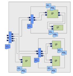
To illustrate how the IJTAG languages are used, consider the simple design shown in Figure 1. Here five instruments, or IP blocks, have been connected together with paths to a top-level access point shown on the left. Each of the five IP blocks is provided with its own ICL file describing its control interface and a PDL file outlining the operations that can be performed on it. The designer connects these blocks together through a simple network of registers that connect back to a top-level IEEE 1149.1-compliant external test access point (TAP) on the left. The form of these registers and the preferred ways to connect them together are recommended in the IJTAG standard, although these mechanisms are very flexible.
Figure 1. Sample IJTAG Network
Commercial automation tools now exist that can read all the ICL and PDL files included with the IP blocks and verify that each IP block is fully IJTAG compliant. This verification is done by creating test benches to simulate the PDL against each IP block’s Verilog description. Automation also is available to extract ICL descriptions for the interconnecting paths to the top-level TAP from either a gate-level or RTL netlist and to verify that they also are correct and IJTAG compliant.
The IP block and extracted ICL descriptions then are used to merge and retarget the instrument PDL procedures so that all the operations provided for each instrument can be controlled from the top-level TAP. From the user’s perspective, causing an operation to happen in any selected instrument is simply a matter of writing a command to the instrument in the top-level PDL. Pattern translations, merging, and routing happen automatically.
Automation also exists to translate the top-level PDL into other types of patterns, such as test vectors to be applied to the top-level TAP from ATE.
IEEE P1687 and 3-D IC Testing
The IJTAG standard is quickly becoming a key component in addressing the growing requirement of testing 3-D stacked devices. One of the basic test challenges with these devices relates to test access. In a 3-D stack, typically only the bottom die has its I/Os bonded to the package pins. All other dies are only connected to their direct neighbors (top or bottom) through TSV connections. Routing test data to and from any of these dies therefore requires some infrastructure for passing test data from one die to the next. Although in principle this is relatively straightforward, the challenge lies in the fact that a stack generally will contain dies from different sources. Mechanisms for passing test data within each die must, of course, be compatible so standardization is needed.
Fortunately, the P1838 working group currently is developing such a standard. The goal of this standard is to describe a test access architecture that supports the necessary vertical transportation of test-related data across multiple dies. However, the standard does not provide a language to describe a particular implementation of the architecture. This is where IJTAG fits in. The flexible and hierarchical nature of the IJTAG standard makes it perfectly suited for describing the details of the access architecture.
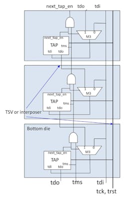
The basic architecture being developed by the P1838 working group consists essentially of enhanced daisy-chained TAPs—one in each logic die, as illustrated in Figure 2. This approach offers the following benefits:
- Each die remains fully 1149.1 compliant. Any tests generated using the standard interface still can be used.
- Each TAP is still fully effective even if the die is packaged as a standalone part.
- The TAP structure supports any die position in the stack so a die can be designed independent of vertical stack position.
Figure 2. 3-D IC TAP Structure
Each enhanced TAP contains additional routing logic and instruction bits to support the new 3-D transport requirement. The TAPs and their connectivity can be fully described using ICL, and the specification of the various 3-D test modes can be defined in PDL.
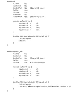
To illustrate the IJTAG standard’s effectiveness in supporting 3-D test architectures, consider the sample ICL and PDL code (Figure 3) for the example stacked dies architecture shown in Figure 2. Assuming the TAP module already has been defined, the ICL descriptions for each die are shown in Figure 3. All dies are described identically except for the topmost die because it has no connection to a higher level die.
Figure 3. Sample ICL and PDL Code for a Stacked Die Architecture
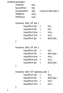
Given the die-level ICL descriptions, the 3-D stack then can be described using the simple ICL code shown in Figure 4.
Figure 4. ICL Code Describing a 3-D Stack
The simple PDL code (Figure 5) then can be applied to the ICL in Figure 4 to configure the network. More precisely, this example PDL puts the lower two dies into operation mode Bypass Scan/External Scan Through and configures the top-level die for die internal test.
Figure 5. PDL Code Used with ICL Code for Network Configuration
Summary
The growing levels of IP integration in both two and three dimensions require new standards and automation solutions to ensure cost-effective design effort and schedules. The upcoming IEEE P1687 standard will no doubt play a critical role in addressing the test- and debug-related aspects of these integration challenges.
About the Author
Stephen Pateras is product marketing director for Mentor Graphics Silicon Test products. Previously, he was the vice president of marketing at LogicVision, and from 1991 to 1995, held various engineering lead and management positions within IBM’s mainframe test group. Pateras received a Ph.D. in electrical engineering from McGill University. [email protected]
For More Information
About the Author
Voice Your Opinion!
To join the conversation, and become an exclusive member of Electronic Design, create an account today!

Leaders relevant to this article:


