Characterizing Leakage Current of High-Voltage Semiconductor Devices

Growing concerns about energy efficiency have led to the development of electronics with higher power density. In grid-connected and industrial applications, such as AC motor control, uninterruptible power supplies, and traction control (large hybrid and electric transport vehicles), the need to keep manageable cable sizes pushes power conversion to higher voltages.
Historically, the semiconductor device of choice for such voltages has been the thyristor. However, recent technological advances in device fabrication and material processing are making possible the development of IGBTs and MOSFETs rated to handle thousands of volts. Wherever possible, using IGBTs or MOSFETs in place of thyristors permits power conversion at high switching frequencies. The migration to higher frequency reduces the size of passive components used in the design and, thereby, improves energy efficiency.
Basic characterization of high-voltage semiconductor devices typically involves a study of the leakage current, which can help a device designer determine quickly if the device was manufactured correctly and if it can be used effectively in the target application.
Leakage current measurements
Leakage current is the level of current that flows through two terminals of a device even when the device is off. It factors into the standby current of the end-product. In most cases, temperature and the voltage across the terminals of interest will affect leakage current. Minimizing leakage current minimizes power loss when the device is off. This power is consumed by the device and is not output to the load; therefore, it contributes to power inefficiency.
When using a transistor or diode to switch or rectify, it’s important to make a clear distinction between ON and OFF states; therefore, a lower leakage current means having a better switch. Also, when evaluating the reliability of a device, leakage current measurements are used to indicate device degradation and make predictions of device lifetime.
While testing a device’s OFF state, generally it is desirable to test the gate leakage current and drain or collector leakage current. For power devices, these values typically are within the nanoamp and microamp ranges so they can be measured using the sensitive current measurement capability of SMU instruments. This capability can be greatly beneficial when testing devices made of wide bandgap materials such as silicon carbide, gallium nitride, and aluminum nitride, which typically have lower leakage currents than do silicon devices. Figure 1 is a plot of OFF-state drain voltage vs. drain current results for a commercially available SiC power MOSFET.

To test devices at extremely high voltages (>3 kV), a high-voltage power supply is needed. Although most power supplies have some current measurement capabilities, semiconductor researchers are investigating materials intended to make higher quality switches and produce devices with very small leakage currents. Such currents may fall below the measurement capability of high-voltage power supplies. In such cases, often the best solution is to couple the accurate sourcing capability of the power supply with the precision low-current measurement capability of an SMU instrument optimized for low current measurements. This approach not only improves the system’s low current measurement resolution and accuracy, but also improves the accuracy of the current limit.
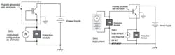
Figure 2 illustrates the high-voltage diode leakage current measurement results obtained using the test setup shown in Figure 3. The diode has a maximum specified reverse current of 10 µA when 3,300 V is applied at room temperature. The results show that the diode meets its specification. The reverse current grows at a faster rate as the reverse voltage increases, indicating that the diode is approaching breakdown.

Voltage is applied with a 5-kV power supply, and current is measured with an SMU instrument.

Figure 4 shows the results of the collector-emitter cutoff current measurement of a 4,000-V IGBT. In this test, the gate and emitter terminals are shorted to ensure that the device remains off (Figure 5a). An SMU instrument also can be used to program the gate voltage. Using an SMU instrument is useful if it’s desirable to make leakage current measurements with the device in hard cutoff (with a bias less than 0 V at the gate terminal). Figure 5b depicts the setup using two SMU instruments and one high-voltage power supply.

The short between the gate and emitter terminals keeps the device in the off-state.
Figure 5b. Test setup (right) using a high-voltage power supply and two SMU instruments to measure the cutoff current (ICES) of an IGBT
The SMU instrument connected to the gate terminal can be used to place a certain bias on the gate, for example, to drive the device into hard cutoff.
This particular IGBT has a maximum specified cutoff current of 100 µA at 4,000 V. The performance of this IGBT is much better than the specification. In fact, even at 4,500 V, the cutoff current isn’t increasing rapidly, which indicates the device isn’t yet in breakdown. The command sequence to generate the results shown in both Figures 4 and 5using a high-voltage power supply and an SMU instrument are included in Keithley Application Note #3249.
Measurement considerations
System validation is crucial for low-current characterization to ensure the measurement is settled. Settling time increases as the expected current decreases. Look for SMU instruments that have auto delay settings that set reasonable delays to achieve good measurements while taking the instrument’s settling characteristics into account. However, to account for any unguarded system capacitance, perform a measurement validation by stepping voltage and measuring the resulting current through the system. Use the results from the validation to set additional source and measure delays to achieve consistent measurements.
To prevent unwanted measurement error when measuring currents less than 1 µA, use triaxial cables and electrostatic shielding as much as possible between the device under test and the SMU instrument. Triaxial cables are essential in part because they permit carrying the guard terminal from the current measurement instrument. Guarding eliminates the effect of system leakage currents by routing them away from the measurement terminal. Use an electrostatic shield to shunt electrostatic charges away from the measurement terminal. An electrostatic shield is a metal enclosure that surrounds the circuit and any exposed connections. The safe test enclosure may serve as an electrostatic shield.1
Safety considerations
High-voltage testing requires exercising extreme caution to protect both operators and test system hardware from danger. As a part of a system safety review, consider all potential consequences of device failure. In a setup that employs both a high-voltage power supply and an SMU instrument, a device breakdown could result in high voltage appearing at the input terminals of the SMU instrument. However, the SMU instrument isn’t designed to handle these higher voltages, so it must be protected against possible damage by the high-voltage power supply.
Protection modules have been developed precisely for this purpose. For example, the Keithley Model 2290-PM-200 Protection Module can be used to protect a Model 2636B SMU instrument from damaging voltages that could be inadvertently output when either a Model 2290-5 5-kV or a Model 2290-10 10-kV high-voltage power supply is used in the test circuit (see Figure 3).
In addition to the use of a protection module, follow these precautions to ensure that the operator won’t be exposed to unsafe voltages:
- Enclose the DUT and any exposed connections in a properly grounded fixture.
- Some power supplies can generate up to 10 kV, so always use the power supply’s safety interlock. Some of the newest models are fully interlocked so that the high-voltage output is turned off if the interlock isn’t engaged (interlock switch closed). To ensure that operators don’t come in contact with a high-voltage connection to the DUT, the interlock circuit of the power supply should be connected to a normally open switch that closes only when the user access point in the system is closed. For example, opening the lid of the test fixture should open the switch/relay that disengages the interlock of the power supply.
- Some SMU instrument are capable of generating voltages up to 200 V, so they also need to have a safety interlock to ensure operator safety during changes in the test setup. For optimum system safety, the interlock of the SMU instrument should be wired in parallel with that of the high-voltage power supply.
- Use cables and connectors rated to the maximum voltage in the system. Look for power supplies that include appropriately rated accessories that the test system designer can use to interface to the DUT.
For more information
1. Low Level Measurements Handbook, Keithley Instruments, 7th Edition.
About the author
Jennifer Cheney is a staff applications engineer at Keithley Instruments, which is part of the Tektronix test and measurement portfolio. She earned a B.S. in electrical engineering from Case Western Reserve University. She has been assisting Keithley customers with instrument applications since 2001. [email protected]
About the Author
Comment About the Article
To join the conversation, and become an exclusive member of Electronic Design, create an account today!

Leaders relevant to this article: